The ability to reduce energy loss at semiconductor surfaces through passivation or surface field engineering is an important step in the fabrication of high-efficiency photovoltaic (PV) and optoelectronic devices. Likewise, surface modification of emerging halide perovskites with quasi-two-dimensional (2D) heterostructures is now ubiquitous to achieve photovoltaic power conversion efficiencies (PCE) >25%, but there are still many questions about how these processing capabilities work. Basic understanding is still generally lacking.
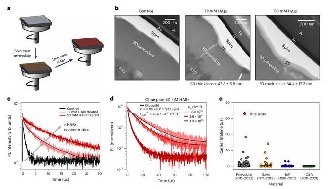
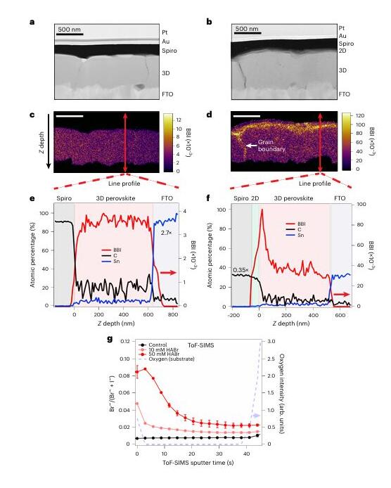
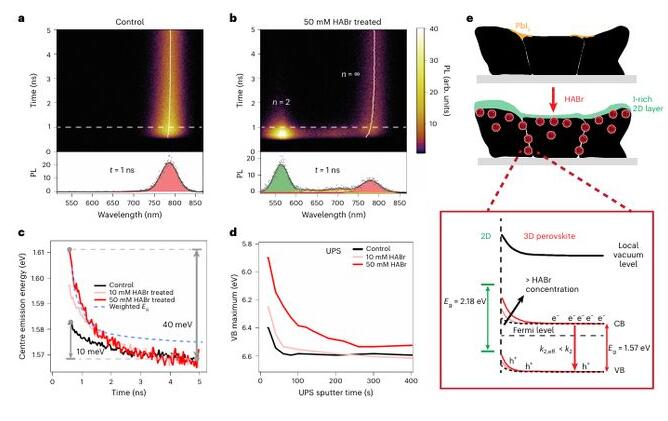
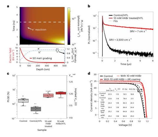
Here, MIT Moungi G. Bawendi & Vladimir Bulović & Korea Institute of Chemical Technology Seong Sik Shin et al. use a unique combination of depth-sensitive nanoscale characterization techniques to reveal tunable passivation strategies found in perovskite photovoltaic devices and mechanism, these devices are the first to achieve the >25% PCE milestone. That is, treatment with hexalammonium bromide results in the simultaneous formation of an iodide-rich two-dimensional layer and a Br halide gradient extending from defective surfaces and grain boundaries to the bulk three-dimensional (3D) layer. The interface can be optimized to extend the charge carrier lifetime to record values >30 μs and reduce the interfacial recombination velocity to as low as <7 cm s −1.
deQuilettes, DW, Yoo, JJ, Brenes, R. et al. Reduced recombination via tunable surface fields in perovskite thin films. Nat Energy (2024).
https://doi.org/10.1038/s41560-024-01470-5
 E-mail: info@chemborun.com
 Tel: +86-574-87178138
  No. 1558, Jiangnan Road,, Ningbo, Zhejiang, China (Mainland)/31