The translation of the provided text
1. Summarized the latest research developments in the stability of perovskite-silicon tandem solar cells (TSCs).
2. Clarified the key degradation mechanisms unique to the cell and module levels, including considerations of perovskite phase separation and the impact of stress on stability. Additionally, discussed new challenges faced by perovskite thin films on textured surfaces and with TSC-specific electrode designs, as well as degradation effects due to current matching constraints.
3. Determined, based on economic factors, the required lifetime energy output for perovskite-silicon TSCs to compete with single-junction silicon solar cells.
4. Finally, outlined the critical future research directions necessary to achieve long-term stability for the successful commercialization of this promising TSC technology.
Background Overview
Despite the proven high-efficiency potential of perovskite solar cells (PSCs), stability is widely regarded as a critical bottleneck hindering the commercialization of PSCs in both tandem and single-junction configurations. The stability progress of perovskite-silicon tandem solar cells (TSCs) lags behind that of single-junction devices. This is because the challenges faced by perovskite-based tandem structures not only stem from the inherent stability issues of PSCs themselves but also from factors associated with the tandem configuration, including charge transport layers (CTLs), encapsulation methods, and operating conditions. Currently, there is a lack of standardized stability testing protocols for tandem devices, making it difficult to directly compare reported stability results and hindering the elucidation of critical degradation mechanisms.
Stability Testing Standards
IEC: To obtain commercial certification for photovoltaic technology, compliance with the IEC 61215 standard is required (see Article SI for details). These specifications define a series of interconnected stress tests that can accelerate the aging process of photovoltaic modules under various stress conditions. In order to compete on an industrial scale, perovskite-silicon tandem solar cells must meet at least the IEC 61215 standard, ensuring that they operate with an efficiency decay of no more than 80% after 25 years.
ISOS: Considering the unique characteristics of perovskite materials, particularly ion migration, which can lead to reversible and irreversible changes in power output, the evaluation of stability using traditional IEC standards becomes complex. The consensus within ISOS has redefined new testing methods related to PSC properties. IEC has recognized the importance of this and is currently considering incorporating stability tests based on ISOS protocols into updated IEC standards.
Establishment of Stability Databases: Researchers are encouraged to adopt standardized stability testing and have their state-of-the-art stability results independently verified by third-party organizations. Simultaneously, these verified stability data should be uploaded to solar cell performance databases based on perovskite technology, such as https://www.perovskitedatabase.com/
Accelerated Aging Tests
Light Soaking Aging: Progress in stability testing under illumination for tandem devices has been relatively limited, and there is currently a lack of stability tests that conform to IEC standards. Performance losses under illumination conditions can be mitigated by optimizing interface layers, and there have been promising developments in interface optimization between perovskite and C60.
Damp Heat Testing: Studies on the stability of perovskite-silicon tandem solar cells are relatively rare, while single-junction perovskite solar cells have shown good damp heat stability. Improved methods, such as the introduction of carbonyl azide heterocyclic compounds, can enhance damp heat stability. Under damp heat conditions, interface tuning between CTLs and perovskite is also an important factor influencing stability. Additionally, damp heat testing can challenge the performance of encapsulation methods.
Real-World Testing
While accelerated tests aim to simulate years of real-world exposure, experience in the silicon industry has shown that these tests often fall short of accurately replicating long-term actual exposure. Therefore, the ultimate test of device performance lies in long-term field testing. For tandem cells, the solar irradiance spectrum varies throughout the day, year, and at different locations, leading to current mismatch issues between top and bottom cells in a 2-T tandem structure, which can affect long-term stability.
Implementation Example: In the hot and dry climate of Saudi Arabia, long-term (approximately 7 days) outdoor stability testing was conducted on a 25% efficient 2-T bifacial perovskite-silicon tandem solar cell, demonstrating that high temperatures caused current mismatch in 2-T perovskite-silicon TSCs. After six months of outdoor testing on a 23% efficient 2-T perovskite-silicon TSC, the open-circuit voltage (Voc) remained unchanged, but the fill factor continuously decreased from the initial value of 0.8 to about 0.5. The degradation mechanism of the fill factor is related to ion migration in perovskite and is largely reversible overnight but exhibits hysteresis over time. Furthermore, long-term irreversible degradation is attributed to the formation of silver iodide (AgI) due to the corrosion of the top silver electrode, highlighting the importance of designing more stable electrode structures for perovskite-silicon TSCs. Devices encapsulated with a novel carbonyl-additive inhibited perovskite layer phase separation and maintained 28.2% of the initial output after 40 days of outdoor testing.
Current Status and Future Outlook: Stability testing of perovskite-silicon TSCs is still in its early stages. Currently, the lifetimes of the most advanced perovskite-silicon TSCs still lag significantly behind silicon devices. Moreover, most research focuses on single or dual stress factors. While some reports have proposed methods to improve the stability of perovskite-silicon TSCs, the field still lacks a systematic understanding and standardized approaches. To advance our understanding of degradation mechanisms in perovskite-silicon TSCs, more systematic and comprehensive analyses are needed, including extended multi-stress factor accelerated tests and large-scale outdoor testing.
Degradation Mechanisms in Perovskite-Silicon Tandem Devices
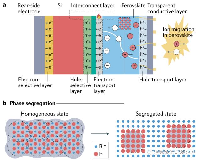
Overall Analysis: Perovskite materials are composed of a soft lattice structure and serve as effective electronic conductors. However, they also contain defects such as vacancies and interstices, forming a conductor for mobile ionic defects. Ionic migration has a low activation energy (e.g., reported values for I- migration range from 0.1 to 0.3 eV). Ionic migration leads to localized chemical stoichiometric changes, resulting in the degradation of perovskite materials. For example, due to the migration of organic and halide ions, Pb2+ ions can be reduced to metallic Pb0 defects, increasing non-radiative recombination effects in perovskite solar cells. At the device level, mobile ions from the perovskite layer can migrate into charge transport layers and electrodes, reducing their charge transport and extraction performance. Ionic migration is considered a core element in many degradation mechanisms. For instance, in wide-bandgap perovskites, phase separation is a consequence of ionic migration.
Phase Separation in Wide-Bandgap Perovskites: In addition to the degradation caused by the intrinsic phenomenon of photo-induced phase separation in mixed wide-bandgap perovskites like IBr, there are adverse effects on charge transport. Changes in the optical bandgap can lead to mismatched photocurrents between the top perovskite cell and the bottom silicon cell, thereby adversely affecting device stability, especially when the series current is limited by the silicon cell.
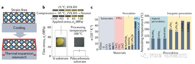
Strain: Perovskites typically exhibit a relatively high coefficient of thermal expansion (CTE), ranging from 3.3 to 8.4×10^-5 K^-1, whereas silicon has a CTE of approximately 0.26×10^-5 K^-1. Therefore, during cooling, the silicon substrate restricts the contraction of the perovskite. Due to the larger CTE mismatch in perovskite-silicon tandem solar cells (TSCs) compared to the CTE mismatch between the perovskite layer and substrate in single-junction PSCs, perovskite thin films experience higher stress under temperature or humidity and degrade more rapidly. Besides tensile and/or compressive strains related to the substrate, grain boundaries, lattice distortions, and non-stoichiometric distributions within the perovskite film have also been identified as sources of localized lattice strain.
<p><br></p>Strain in Perovskite Films also depends on the film deposition process. In solution-based processing, local environmental changes due to post-annealing treatments, solution concentration gradients, and the presence of intermediate complexes can lead to heterogeneous growth of polycrystalline films, generating numerous grain boundaries. Additionally, the texturing of the silicon substrate enhances the stress in the perovskite film. Most perovskite materials used for solar cells have relatively low thermal conductivity, typically below 0.50 W(mK)^-1 (e.g., MAPbI3 and CsPbI3 have thermal conductivities of 0.34 and 0.45 W(mK)^-1, respectively, at room temperature). Therefore, during operation, the steady-state temperature in the perovskite layer exacerbates thermal stress, impairing device stability. Addressing the mismatch in coefficient of thermal expansion (CTE) between materials in perovskite-silicon TSCs is crucial, and it involves altering annealing processes, such as lowering crystallization temperatures, to avoid large residual strains in the perovskite film. Furthermore, interface management, including selecting CTLs with better-matching TEC properties, is necessary. However, CTLs also need appropriate optoelectronic properties to ensure efficient charge extraction.
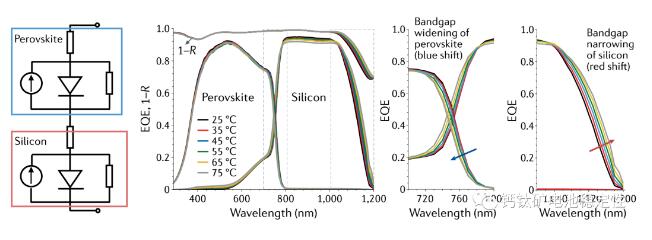
Current Matching: In 2T perovskite-silicon TSCs, the total photocurrent depends on the lower photocurrent of the two sub-cells. Therefore, a high and balanced photocurrent is necessary for maximum power generation. Photocurrent mismatch, in turn, leads to other instabilities in 2T perovskite-silicon TSCs. Especially when the silicon sub-cell performs poorly, such as in overcast or cold weather, the perovskite sub-cell will be pushed toward V_oc at lower photocurrents, increasing the charge carrier density and, thus, accelerating phase separation. In real-world operation, variations in temperature and light intensity occur daily and seasonally, along with changes in the solar spectrum. With increasing temperature, the bandgap of perovskite increases while that of silicon decreases, leading to photocurrent mismatch in actual operation. However, this effect may be smaller than anticipated, as observed MPP currents for perovskite and HJT devices remain relatively stable under elevated temperature and irradiance conditions. At low light intensities, the PCE of PSCs decreases less compared to HJT, and in the range of 0.5-1.0 sun, where most power generation occurs, the differences are not critical.
In addition to phase separation and strain, degradation mechanisms in perovskite-silicon tandem devices also include the following two points:
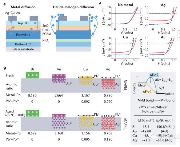
Electrode Design: For perovskite-based solar cells, widely used metal electrodes such as Au or Ag can introduce instability by diffusing into the perovskite and forming shunt paths, especially at higher temperatures. In particular, Ag can react rapidly with halogen species in the perovskite to form silver halide, leading to irreversible device degradation. The electrode design for perovskite-silicon TSCs differs from that of single-junction devices as it requires high transparency within the photon energy range below the perovskite bandgap to maximize light absorption in the silicon bottom cell. So far, the most effective transparent electrodes in dual-contact structure devices rely on thin-layer sputtered transparent conductive oxides (TCOs) with metal grids for charge collection. Combining TCOs with front grids reduces metal coverage and mitigates electrode-induced degradation. Transparent electrodes are also more suitable for industrially relevant encapsulation techniques, as they can protect the device from damage during the encapsulation process. To prevent sputter damage to the underlying layers, an inorganic buffer layer is often introduced before TCO deposition. For example, p-i-n and n-i-p TSCs use atomic layer-deposited tin oxide (SnOx) and thermally evaporated molybdenum oxide (MoOx), respectively. Dense SnOx layers deposited by ALD have been reported to protect 2T perovskite-silicon TSCs from moisture infiltration, thereby improving stability. In contrast, MoOx layers can wrinkle and delaminate at elevated temperatures or even at room temperature due to their low crystallization temperature and high sensitivity to moisture, limiting device stability.
Iodide Transport: The transport of iodide in the form of volatile species, especially at the edges of PSCs, is an important degradation mechanism. Iodide silver (AgI) has been observed on the top surface of semi-transparent perovskite devices, but not in charge transport layers, anti-reflection coatings, or electrode layers, indicating that iodide may not migrate through permeation but likely originates from the edges of the device. Blocking the edges of the active layer and introducing barrier layers are effective strategies to prevent the escape of volatile species. It has been reported that ALD layers, whether embedded within the cell or placed on top of the entire cell, can inhibit the migration of iodide because they have high density.
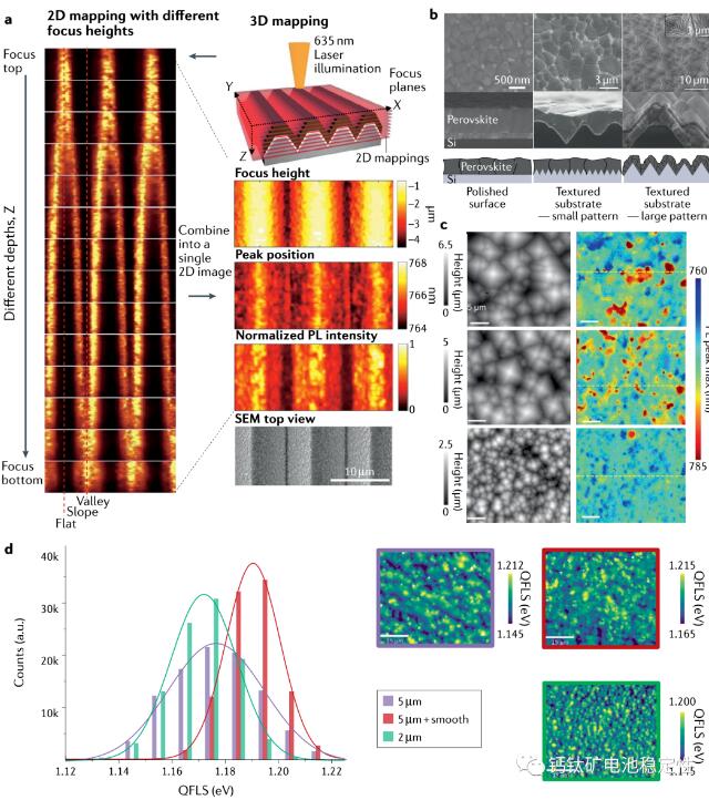
Surface Texturing of Silicon Cells: Surface texturing, along with the deposition method of perovskite, jointly determines the growth kinetics, morphology, crystallinity, strain, and uniformity of perovskite, all of which have important implications for device stability. Studies on the relationship between texture and perovskite film quality on V-groove textured devices have revealed that the photoluminescence (PL) peak shifts to the blue and has lower intensity when measured at non-planar substrate locations (such as edges and valleys on a flat surface). The PL shifts on substrates with different morphologies could be attributed to strain or local compositional changes. Correspondingly, the current output at the tips and valleys of V-groove textures is relatively lower. Similarly, in high-performance textured perovskite-silicon TSCs research:
There is a strong correlation between PL intensity and spectrum with the geometric shape of the texture. When pyramid sizes are small, PL distribution becomes more uniform. In large-sized (pyramid height of 5 μm) texture schemes, the PL spectra in valleys and pyramids are different, and most of the spatial intensity and spectral PL heterogeneity can be attributed to increased light absorption in the valleys of the pyramids.
The size of the quasi-Fermi level splitting also varies with texture design. For example, perovskites on different pyramid sizes (5 or 2 μm) on silicon show similar quasi-Fermi level distribution peak positions, while additional smoothing etching not only improves PL uniformity but also significantly improves the quasi-Fermi level. These studies demonstrate the complex relationship between texture geometry and the uniformity, strain, and morphology of the generated perovskite film, which affects the phase stability of TSCs.
The depletion region in the perovskite is much wider at the bottom of silicon pyramids (approximately 380 nm) compared to the top (approximately 120 nm). The depletion region is wider at the HTL-perovskite interface compared to flat perovskite cells, while it remains similar at the ETL-perovskite interface (top). This observation suggests that the depletion layer width is the largest where the perovskite is thickest, which facilitates efficient charge collection. As excess charge in the perovskite sub-cell can stimulate defect formation and ion migration, this larger depletion width can enhance series efficiency and stability. Further long-term stability testing of perovskite-silicon TSCs on substrates with different textured sizes is still needed to fully understand the impact of texture on device stability.
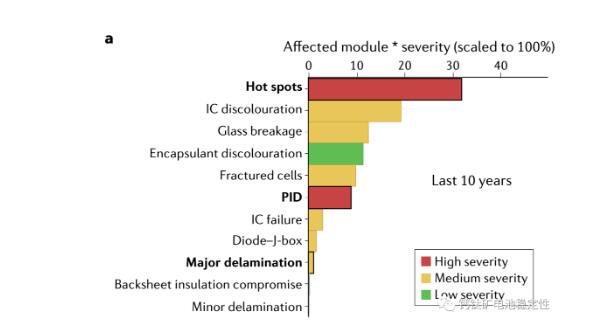
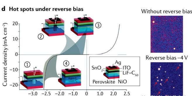
Reverse Bias Voltage and Hot Spot Effects: Currently, the mechanisms behind the characteristics and stability of perovskite-silicon tandem solar cells (TSCs) under reverse bias (RB) conditions are not fully understood. In traditional semiconductor solar cells, a sufficiently large RB voltage can lead to breakdown, resulting in a significant reverse current. Ideally, RB breakdown current is evenly distributed across the entire cell, but spatial non-uniformities or local defects can lead to isolated areas with lower breakdown voltages, triggering destructive localized Joule heating. Such hotspots have been directly observed in single-junction perovskite devices, indicating the importance of material uniformity in withstanding RB conditions. Tandem devices may be more susceptible to forming hotspots.
First, sharp edges in tandem devices can concentrate the electric field, causing localized current flow even in the top perovskite cell deposited on textured silicon, even in ideal conditions. Second, localized heating in the c-Si bottom cell, while acceptable in single-junction c-Si devices, may be detrimental to the top perovskite cell due to the significant differences in thermal stability between the two materials. For example, under 2T and 4T conditions, the actual hotspot temperatures beneath the shading modules reached as high as 207°C and 137°C, respectively, both exceeding the known decomposition temperature threshold for mixed-halide perovskites. The electrode may play a crucial role in resisting hotspots, as perovskite solar modules using carbon-based electrodes have passed the "hotspot" test described in the IEC 61215 standard.
In addition to thermal hotspot damage, ion migration can lead to power losses under reverse bias (RB) conditions. Incomplete power recovery is attributed to ion accumulation at the device interfaces, stimulating electrochemical reactions at RB of -4V. Ion migration within the perovskite is observed after RB, with ions even migrating into the ETL. A temporary reduction in photocurrent at MPP is observed when RB is lowered to -1.1V, causing shaded cells to remain in an RB state after shading is removed.
Voltage-Induced Degradation: Typical photovoltaic system modules in a series configuration result in an end-to-end potential difference of 1,000V, with the first and last modules having the highest potentials at +500V and -500V, respectively. This potential difference can lead to a well-known power loss phenomenon called Potential-Induced Degradation (PID). In silicon photovoltaics, PID effects depend on various factors such as the quality of encapsulation and encapsulation materials, characteristics of anti-reflective coatings, system configuration (system voltage, use of inverters and transformers), environmental stress factors (humidity, condensation, and temperature), module structure (framed or frameless), and grounding conditions on the glass surface (wet or dry). PID is caused by alkali metal ions (such as sodium ions Na+) migrating from surface layers, including the glass cover, into the silicon wafer. These effects may be destabilizing for silicon-silicon tandem cells. Challenges for long-term stability are related to the migration rates of many constituent elements of perovskite cells, and suitable charge transport layers (CTLs) or perovskite compositional engineering can address this to some extent.
Interlayer Separation: Tandem devices consist of multiple layers of materials, and interlayer separation due to thermal expansion coefficient mismatches during thermal cycling has been observed. Layer separation has been observed between the PCBM layer and PTAA with perovskite in single-junction PSCs and 2-T perovskite-silicon TSCs. Methods to improve this mechanical stability include additive engineering, optimizing interface adhesion, selecting encapsulation materials with lower elastic modulus, and more.
Economic Stability Considerations: The competitiveness of photovoltaic systems in the market can be assessed through the Levelized Cost of Electricity (LCOE), which is influenced by device efficiency and initial costs. For perovskite-silicon TSCs, superior stability is more critical than efficiency improvements or cost reductions to achieve competitive LCOE. Many studies have shown that as the degradation rate increases from 1% per year to 3% per year, maintaining the same LCOE requires at least a 10% absolute efficiency increase or a cost reduction of over 60% in module manufacturing. Therefore, stability is crucial for the commercialization of perovskite-silicon TSCs. Research has also found that as the degradation rate increases, higher efficiency or lower costs are required to maintain the same economic performance. The specific LCOE for perovskite-silicon TSCs needs to consider factors like stability, and modeling analysis can determine the corresponding LCOE targets.
Outlook:
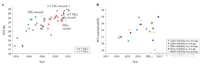
1. Perovskite-silicon TSCs represent the fastest route to market introduction for tandem photovoltaic systems. Significant investments have already been made, achieving a high level of technological readiness within a short span of 10 years, with efficiencies exceeding 30%, and industrial module integration has been validated.
2. Stability issues remain the primary obstacle in the development of perovskite-silicon TSCs. Degradation mechanisms, including ion migration and redistribution, threaten long-term stability and require extensive improvements at small-area and module-level scales.
3. Standardized testing protocols can predict the long-term performance of perovskite photovoltaics, and stricter testing standards are needed to enhance commercial viability.
4. Perovskite-silicon TSCs need to address structural issues such as perovskite film fragility and thermal expansion mismatch while optimizing the surface morphology and optoelectronic quality of the substrate. Phase segregation issues can be addressed using single-crystalline wide-bandgap perovskite quantum dots or inorganic CsPbI3 perovskites.
5. Transparent electrode designs for TSCs can minimize metal diffusion into perovskite films. Suitable material selection and stable buffer layers can prevent metal diffusion and perovskite ion migration.
6. Interface quality plays a critical role in TSC stability, and stable key materials need to be identified. TOPCon technology can provide more material choices and process flexibility.
7. More reliability analysis at the module level is needed to improve the predictability of module failures. The impact of different structures, interfaces, and encapsulation materials on module stability needs to be studied.
 E-mail: info@chemborun.com
 Tel: +86-574-87178138
  No. 1558, Jiangnan Road,, Ningbo, Zhejiang, China (Mainland)/31