The advanced nano-optoelectronic materials and devices team of Ningbo Institute of Materials Technology and Engineering, Chinese Academy of Sciences (hereinafter referred to as "Ningbo Institute of Materials") recently developed an efficient and stable perovskite light-emitting diode with world-leading performance, solving the problem of perovskite materials . The intrinsic stability problem points out the direction for the industrialization of perovskite light-emitting diodes.
On February 5, 2024, this result was titled "Phase dimensions resolving of efficient and stable perovskite light-emitting diodes at high brightness" and was published online in Nature Journal of Photonics.
The Ningbo Institute of Materials is the first unit to complete this achievement and the corresponding unit. Its 2024 fresh doctoral graduate Ding Shuo is the first author, and Xiang Chaoyu and Qian Lei, researchers of the advanced nano-optoelectronic materials and devices team of the institute, are the corresponding authors.
Figure 1: Bright fluorescence of different perovskite materials and perovskite light-emitting diodes under UV light (lower right).
Photo courtesy of the research team
Perovskite materials are currently one of the most promising optoelectronic materials. They have the advantages of excellent optoelectronic properties and low solution preparation costs. Perovskite light-emitting diodes are also considered to be the strongest competition to replace existing OLED technology and become future light-emitting display technology. one of those.
However, although perovskite light-emitting diodes have made significant progress in efficiency for a long time, the problem of low operational stability is still the main reason that hinders their practical use. In particular, the academic community has not understood the fundamental sources that affect the stability of perovskite materials. The understanding is not deep enough, which undoubtedly hinders the further improvement of the performance and commercial application of perovskite light-emitting diodes.
The Advanced Nano-Optoelectronic Materials and Devices Team of the Ningbo Institute of Materials conducted an in-depth analysis of the fine nanostructure inside the representative quasi-two-dimensional perovskite material and found out the thin nanosheets inside - only 1 or 2 layers. Lead ions are a key source of instability in perovskites.
These thinner nanosheets are formed by a rapid and uncontrollable crystallization process. They have poor crystal quality, many defects, and are prone to decomposition. Moreover, their decomposition will further induce the decomposition of the entire perovskite film, greatly reducing the stability of the perovskite material.
Therefore, effective methods must be developed to precisely remove these thin nanosheets. Unfortunately, because the scale of thin nanosheets is on the nanometer scale and they are closely packed with other structures, conventional macroscopic processing methods are difficult to work.
In order to solve this problem, the team was inspired by the process of sieving sand grains of different sizes and creatively developed a "solvent sieve" method to achieve precise screening of nanosheets of different thicknesses and effectively remove thin particles. The nanosheet phase greatly improves the stability and luminescence performance of the final perovskite material.
The "solvent sieve" developed by the team is a combination of polar solvents and non-polar solvents. It takes advantage of the characteristics of thinner nanosheets that are easily soluble in polar solvents, just like adjusting the size of the sieve to control the size of the sieved sand particles. Similarly, by adjusting the proportion of polar solvents, thin nanosheets with only 1 or 2 layers of lead ions can be accurately removed without damaging other structures in the perovskite material.
This method not only significantly improves the luminescence performance and stability of perovskite materials, but also greatly expands the toolbox for manipulating the fine nanostructure of perovskites, paving the way for the future development of perovskites with unique nanostructures and properties. Materials provide a solid foundation.
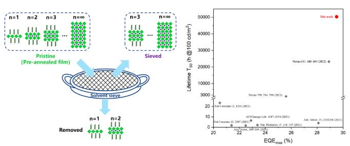
Figure 2: (Left) Schematic diagram of the principle of the "solvent sieve" method; (right) The "solvent sieve" method refreshes the performance record of perovskite light-emitting diodes. Photo courtesy of the research team.
After removing the thin nanosheets through the "solvent sieve" method, the perovskite material showed amazing stability. Not only can it maintain its luminescence performance in humid air for more than 100 days, the prepared perovskite light-emitting diode even showed a luminescence performance of more than 100 days. The operating life of more than 50,000 hours (5.7 years) at candela/square meter brightness is currently the highest value of all green perovskite light-emitting diodes, meeting the requirements for commercial application.
At the same time, the external quantum efficiency of the perovskite light-emitting diode has also reached 29.5%, which is currently the highest efficiency record for perovskite light-emitting diodes designed without light extraction. This research result undoubtedly paves the way for the application of perovskite materials in the field of luminescent displays, greatly accelerating the introduction of perovskite luminescent display devices into thousands of households.
Ding, S., Wang, Q., Gu, W. et al. Phase dimensions resolving of efficient and stable perovskite light-emitting diodes at high brightness. Nat. Photon. (2024).
https://doi.org/10.1038/s41566-023-01372-0
 E-mail: info@chemborun.com
 Tel: +86-574-87178138
  No. 1558, Jiangnan Road,, Ningbo, Zhejiang, China (Mainland)/31