1. Alleviating short device lifetime due to ion migration and low brightness due to severe Auger recombination by in situ solution-grown perovskite single crystals (SCs).
2. By using mixed cations to minimize the trap density and adding excess ammonium halide and povidone in the precursor, the external photoluminescence quantum yield (PLQY) of SCs was increased to 28.3%, corresponding to 89.4% internal PLQY.
3. Thanks to the suppression of Auger recombination in SCs, SC-PeLEDs with a thickness of 1.5 μm exhibit a high luminance of 86,000 cd m−2 and a peak external quantum efficiency of 11.2%. Due to the suppression of ion migration, the extrapolated T50 lifetime of SC-PeLEDs reaches 12,500 h at an initial luminance of 100 cd m−2.
1、 Problems in perovskite light emitting diodes based on polycrystalline (PC) thin films
High external quantum efficiency (EQE) of over 20% has been achieved in perovskite light emitting diodes (PeLEDs) based on polycrystalline (PC) films; This is equivalent to the value achieved by organic LED (QLED) and quantum dot LED (QLED). Recently, the T50 lifetime of green PLEDs with an initial luminance of 100 cd m − 2 (the time required to reach half the initial luminance) exceeded 30000 hours, and the T50 lifetime of near-infrared PLEDs with a current density of 5 mA cm − 2 exceeded 10000 hours. However, their operational stability still lags behind OLED and QLED. Various factors, including ion migration, carrier implantation imbalances, joule heating, electrochemical reactions, and moisture, have been reported to lead to degradation. Ion migration through grain boundaries is considered a major factor in rapid degradation. Although several methods have been tried to suppress ion migration, this issue has not yet been fully resolved. Another problem with PC-PeLEDs is severe rollovers caused by Auger recombination. Due to quantum/dielectric constraints, PC films have a higher exciton binding energy (Eb) than bulk perovskite. In addition, the emissions in PC-PeLEDs mainly come from nanoparticles, whose carrier density is amplified compared to bulk perovskite. These characteristics lead to severe Auger recombination in PC-PeLEDs and limit their maximum available brightness. Perovskite single crystals (SCs) have high carrier mobility, inhibition of ion migration, and Auger recombination. However, due to the low photoluminescence quantum yield (PLQY) of SCs and the difficulty in growing large and thin SCs, there is currently no report on SC-PeLEDs.
2、 Achievement Introduction
In view of this, Xiao Zhengguo's team from the University of Science and Technology of China has used in situ solution grown perovskite single crystals (SCs) to alleviate the short equipment life caused by ion migration and the low brightness caused by severe Auger recombination.
3、 Showing efficient brominated PeLEDs, using thin SCs grown in situ, exhibiting longer operational stability and higher brightness than PC-PeLEDs. Thin SCs composed of methyl ammonium formamide lead bromide (MA0.8FA0.2PbBr3) were directly grown on the hole transport layer using a space limited inversion temperature crystallization (SIC) method.
4、 Results and Discussion
Key point 1: SC-PeLED device growth
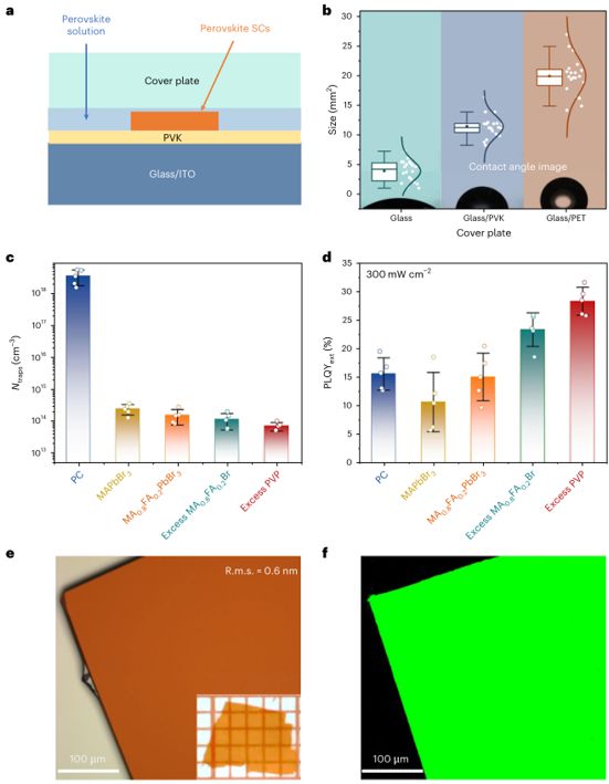
Poly (n vinyl carbazole) (PVK) is an excellent HTL for the preparation of brominated PeLEDs. Therefore, we used the SIC method to directly grow thin perovskite SCs on indium tin oxide (ITO)/PVK substrates (Figure 1a). A hydrophobic cover plate with low surface energy is essential for cultivating large SCs, as it can reduce nucleation density 27 and accelerate ion diffusion to achieve sustained growth of SCs. Using a popular hydrophobic PET as a cover plate, a thin perovskite SCs of~20 mm2 can be obtained (Figure 1b). It is worth noting that compared to PVK, the high hydrophobicity of PET enables it to easily peel off SCs without tearing the crystal surface. The thickness of thin SCs grown by SIC method is generally~4.6 ± 0.7 μ m。 Although the thickness of the SC can be further reduced to~1 by applying pressure to the cover plate μ m. The size of the SC has also been reduced to a few square millimeters (Supplementary Figure 1).
In the optimization process of SC growth, we adopted a method of minimizing the trap density in PC perovskite films (Supplementary Figure 2), using a mixed ion perovskite combination MA1 − xFAxPbBr3 to grow SCs. Add excessive MA0.8FA0.2Br to the precursor solution to reduce the vacancies of organic ammonium or halides in SCs. Adding excessive PVP to the precursor slows down the nucleation process of perovskite and improves its morphology through coordination with Pb-Br complexes. We finally obtained high-quality MA0.8FA0.2PbBr3 perovskite SCs with a trap density as low as~7.1 at a high excitation intensity of 300 mW cm − 2 × 1013 cm − 3, PLQYext as high as~28.3% (Figures 1c, d, and Supplementary Figure 3). Considering the photon escape probability, the PLQYint of SC reaches 89.4% (Supplementary Note 1). For a fair comparison with SCs, we prepared perovskite PC films with the same composition and additives (20% MA0.8FA0.2Br and PVP). The well density of the optimized PC thin film (50 nm) has increased by 5 orders of magnitude, reaching 3.4 × At 1018 cm − 3, PLQYext decreased by 15.7%. Through the above optimized process, high-quality perovskite SCs can be obtained on ITO/PVK substrates. SC has a cubic phase (spatial group Pm3m) structure, crystal orientation<100>(Supplementary Figure 4a), and a very smooth surface (Figure 1e). Scanning electron microscopy (SEM) and atomic force microscopy (AFM) images show that SCs have extremely smooth and grain free surfaces with a root mean square (r.m.s.) roughness of 0.6 nm (Supplementary Figure 5f). Due to the low trap density, sc exhibits very bright and uniform PL emission (Figure 1f). There is a significant PL peak difference between SCs (548 nm) and PC (520 nm) thin films due to their different crystal sizes and the reabsorption of high-energy photons in thick films. It is worth noting that for SCs, the Stokes shift is very small (Supplementary Figure 4b), which leads to photon cycling (PR) effects, reabsorption and re emission of photons. The PR effect can significantly improve the decoupling efficiency of SC-PeLEDs.
Figure 1 Growth and optimization of perovskite SCs
Key point 2: SC-PeLEDs device structure
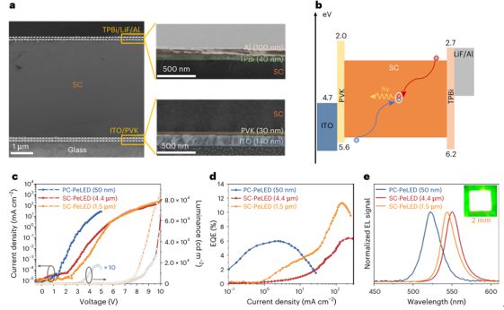
SC-PeLEDs can be prepared by depositing the electron transport layer and the back electrode onto SCs in turn, without any photolithography process. It is worth noting that the PVK layer is not damaged during the growth of SC, as we have done with N, N-dimethylformamide (DMF); The cross-sectional SEM images and energy levels of PeLEDs are shown in Figures 2a and b. It is worth noting that no small perovskite particles were observed on the top or bottom surfaces of SCs, which would reduce the possibility of trap assisted non radiative recombination. The current density voltage luminance (J-V-L) and EQE curves of SC-PeLEDs and PC-PeLEDs are shown in Figures 2c and d. Excitingly, despite the SC's thickness of up to 4.4 μ m. The current density of SC-PeLEDs still reaches~100 mA cm − 2 at 9 V due to the high carrier mobility of 9.84 cm2 V − 1 s − 1 (Supplementary Figure 3f). At low injection current density, the EQE of PC-PeLEDs is higher than that of SC-PeLEDs, because at the same injection current density, PC-PeLEDs have higher Eb and more than 5 times the carrier density (Supplementary Note 2). At high current density, 4.4-m SC-PeLEDs exhibit significant inhibition of slippage compared to PC-PeLEDs, with a high brightness at 216 mA cm − 2 and a peak EQE of 6.4%. By reducing the SC thickness to 1.5 μ m. At 145 mA cm − 2, brightness and EQE increase to 84000 cd m − 2 and 11.2%, respectively, possibly due to reduced reabsorption and improved coupling efficiency in thinner devices.
At a high brightness of 58300 cd m − 2, the current efficiency also reaches 40.4 cd A − 1 (Supplementary Figure 7). The angular spectrum and intensity distribution of the device are shown in Figure 8. The performance of SC-PeLEDs shows good reproducibility (Supplementary Figure 8d). In contrast, the EQE for controlling PC-PeLEDs reached only 5.9% at a much lower current density of 3 mA cm − 2, consistent with recent reports. When the PC thickness increased to 1.5 µ m and 4.4 µ m, the EQE of PC-PeLEDs decreased to 2.5% and 0.5%, respectively (Supplementary Figure 9). As shown in Figure 2e, SC-PeLEDs exhibit very bright electroluminescence (EL), with a redshift emission peak compared to PC-PeLEDs, which is consistent with their PL peak. The high EQE (11.2%) of SC-PeLEDs can be explained by the high PLQYint and PR effects. It is well known that due to the PR effect, photons trapped in waveguide modes can be reabsorbed and re emitted in random directions, which can improve the coupling efficiency of LEDs. Due to the high absorption and PLQYint of the SC layer, PR contributes 82.7% to the total emission in our SC-PeLEDs (Supplementary Note 3 and Supplementary Figure 10), which is equivalent to the most advanced LED based gallium arsenide/gallium nitride (76-90%).
Figure 2 Device structure and performance of SC-PeLEDs.
Point 3: Comparison between SCs and PC films
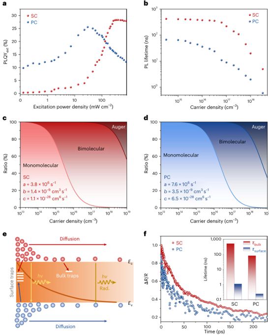
We have studied the differences in carrier recombination kinetics between PC-PeLEDs and SC-PeLEDs, which leads to significant differences in their performance. As shown in Figure 3a, at low excitation intensities, the PLQYext of PC thin films is much higher than SCs, which is due to the higher streamer density and higher photon escape probability of PC thin films at the same excitation intensities (Supplementary Figure 11b). At high excitation intensities, SC exhibits stronger inhibition of roll than PC, which is consistent with the inhibition of EQE roll in SC-PeLEDs. We further investigated the single molecule, bimolecular, and Auger recombination rate constants of PCs and SCs by using excitation intensity dependent transient photoluminescence (TRPL; Figure 3b, Supplementary Figure 12, and Supplementary Note 5). Note that the PR effect affects the rate of radiation recombination because the photons generated by radiation recombination can be absorbed and lead to internal generation of electron holes. We also considered this point (Supplementary Note 5). The ratio of the three recombination terms as a function of carrier density is shown in Figures 3c and d. Single molecule recombination dominates in SCs and PC films with low carrier density (~1014 cm − 3) because a small amount of photogenerated carriers mainly fill traps. Due to the low trap density in SCs, the bimolecular recombination of SCs increases with a lower carrier concentration. It is worth noting that the Auger recombination of PC thin films has a carrier density of 7.0 × 1016 cm − 3, while the carrier density of SCs is~1.3 × 1017 cm−3。 The inhibited Auger recombination in SC was consistent with its lower Eb (23.8 meV), while the Eb (~44.5 meV) of PC membrane was lower (Supplementary Figure 13). Due to the nanoscale grain size, quantum constraints lead to higher Eb values in PC films.
In order to reveal in-depth information on non radiative single molecule recombination in SC-PeLEDs, we investigated the surface carrier dynamics of SCs using transient reflection (TR) spectroscopy. Surface carrier dynamics include surface recombination and carrier diffusion, as shown in Figure 3e. TR spectroscopy detected the carrier dynamics within a few tens of picoseconds after excitation, and there was no mass group at that time. Surface recombination velocity (S) and diffusion coefficient (D) can vary from relative reflectivity( Δ R/R) attenuation curve (Supplementary Note 6 and Supplementary Figure 14). It is worth noting that the non radiative recombination lifetime of the SC surface( τ Surface=1.10 ns) is much shorter than the volume obtained from TRPL results( τ Bulk=511 ns) (Figure 3f). Due to the low trap density of SCs τ Bulk and τ The surface is much higher than the PC film. This result indicates that surface traps are the main non radiative sites in SC-PeLEDs, and surface treatment will be an important way to further improve device performance.
Figure 3 Carrier recombination kinetics of SCs and PC films
Point 4: SC-PeLEDs and PC-PeLEDs run tests
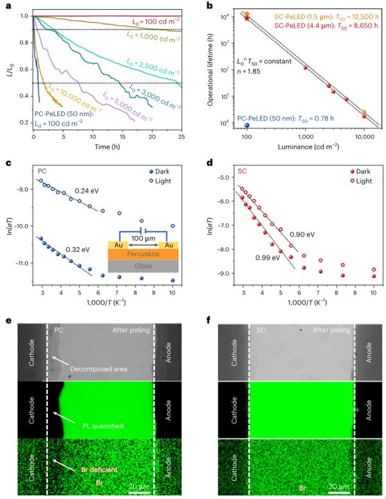
Longer operational stability is another advantage of SC-PeLEDs over PC-PeLEDs. According to the stability characterization criteria in document 17, 4.4 was measured at different initial luminance (L0) from 100 to 10000 cd m − 2 (Figure 4a and Supplementary Figure 15a) μ M The working stability of SC-PeLEDs. The EL peaks of SC-PeLEDs are stable at different aging times (Supplementary Figure 15b), which is understandable because perovskite SC only contains bromine. Using the empirical equation Ln0T=constant, the T50 lifetime of SC-PeLEDs at 100 cd m − 2 is estimated to be 8650 h. It is exciting to note that the T50 lifetime of thinner SC-PeLEDs increases to 2.5 h at an initial brightness of 10000 cd m − 2 (Supplementary Figure 15c), which corresponds to an inferred T50 lifetime of 12500 h at an initial brightness of 100 cd m − 2, possibly due to reduced Joule heating. In contrast, the T50 lifetime of PC-PeLEDs at 100 cd m − 2 is only 0.78 h (Figure 4b), which is comparable to the reported value using three-dimensional organic-inorganic hybrid lead bromide perovskite (Supplementary Table 1). Generally, all inorganic perovskite based PeLEDs have longer operational stability than PeLEDs using organic-inorganic hybrid perovskite due to their more stable structure. From the above perspective, the operational stability of SC peleds can be further improved through composition engineering and reducing SC thickness. It is worth noting that SC-PeLEDs also exhibit inhibition hysteresis on the J-V and EQE curves, which is a sign of inhibition of ion migration in SC-PeLEDs (Supplementary Figure 16). We measured the ion migration activation energy (Ea) in SCs and PC films using a transverse device structure. As shown in Figures 4c and d, the Ea value of SC is 0.99 eV under dark conditions and 0.90 eV under light conditions; These values are several times the value of a PC. The difference in ion migration between SCs and PC films can be directly observed when the transverse device is polarized under an electric field of 2.0 V µ m − 1 for 4 hours. As shown in Figure 4e, PC devices exhibit a significant degradation region near the cathode, where PL emissions are quenched. Energy dispersive spectroscopy (EDS) plots show a lack of Br near the cathode, further demonstrating the migration of Br ions under an electric field. In contrast, no degradation of SCs caused by ion migration was observed after the polarization process (Figure 4f). This is understandable because ions mainly migrate through grain boundaries and defects. SC without grain boundaries and with low defect density has a high ion migration barrier. Therefore, it is reasonable to conclude that inhibiting ion migration is the main reason why SC-PeLEDs improve operational stability.
Figure 4 Operating Stability of SC-PeLEDs and PC-PeLEDs
5、 Summary
In summary, we use the SIC method to directly grow perovskite SCs on HTLs. Through component engineering, adding additives, and controlling the growth process of SC, PLQYint has been significantly increased to nearly 90%. Due to inhibition of ion migration and Auger recombination, SC-PeLEDs have significantly better operational stability and brightness than PC-PeLEDs. It is worth noting that the thickness of our SC-PeLEDs is about a few microns, which is still much thicker than PC-PeLEDs. It is expected that the performance and stability of SC-PeLEDs can be further significantly improved by reducing the SC thickness. New methods for growing ultra-thin SCs, such as chemical vapor deposition and wet etching of thick SCs, will be very attractive.
6、 References
Highly bright and stable single-crystal perovskite light-emitting diodes
https://www.nature.com/articles/s41566-023-01167-3#additional -information
 E-mail: info@chemborun.com
 Tel: +86-574-87178138
  No. 1558, Jiangnan Road,, Ningbo, Zhejiang, China (Mainland)/31