First author: Erkan Aydin
Corresponding author: Erkan Aydin, Stefaan De Wolf
Correspondence unit: King Abdullah University of Science and Technology (KAUST), Saudi Arabia
Article highlights:
To surpass the power conversion efficiency of the best single-junction silicon solar cells, tandem perovskite-silicon solar cells tune the perovskite
layer to absorb the high-frequency end of the solar spectrum to compensate for the silicon cell's absorption deficit. However, for this series power technology to be widely adopted, its levelized cost must be lower than mainstream silicon technology. This article provides a systematic review of the work required to commercialize these devices, including issues such as stability, process scale-up, throughput, cell-to-module integration, and field performance evaluation.
1. Introduction to perovskite/silicon double junction tandem solar cells
Photovoltaic technology is expected to play a key role in curbing the expected catastrophic effects of climate change due to good cost competitiveness, continued technological advancement, and abundant solar resources. For many years, practical deployment of photovoltaic technology has relied on monocrystalline silicon solar cells; however, this technology is now approaching practical efficiency limits. To overcome these limitations and realize the full potential of photovoltaic technology, perovskite/silicon double-junction tandem solar cells have emerged as a promising solution to combine high photoelectric conversion efficiency with cost-effective manufacturing. When first introduced in 2013, initial perovskite/silicon tandem cells performed mediocrely. However, through unremitting research and development efforts, perovskite/silicon tandem cells have now achieved certified photoelectric conversion efficiencies of over 33% on laboratory-scale devices, which is already higher than the theoretical limit of any single-junction cell technology. With significant efficiency potential and the prospect of further improvements, perovskite/silicon tandem cells are now on the road to commercialization.
2. Introduction to results
The team of Erkan Aydin, Stefaan De Wolf from King Abdullah University of Science and Technology in Saudi Arabia reviews the remarkable progress made in translating laboratory-scale tandem performance into industrial-grade modules. Sustainability and raw material costs were also considered key considerations for large-scale production. The most critical efforts required to move toward commercialization lie in improving device stability and performance evaluation in real-world deployment environments. For perovskite/silicon tandems to become a commercially viable option, it is critical to reduce the levelized cost of electricity (LCOE) to a level that is competitive with market-established silicon PV. While higher performance modules have advantages in lowering cost per watt, uncertainty around module durability, energy yield and reliability with emerging photovoltaic technologies such as perovskites may offset the move to lower LCOE . These uncertainties will also hurt the bankability of perovskite/silicon tandem technology. Therefore, accelerated degradation testing specifically for perovskite technology and outdoor testing with accurate energy yield predictions will help drive market entry for this technology.
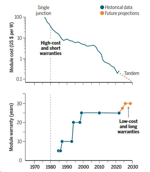
Evolution and forecast of PV module costs and warranty periods over time
3. Content and discussion
Crystalline silicon (c-Si)-based photovoltaic technology, which currently dominates the market, is approaching its theoretical and technical PCE limits. Today, the PCE of c-Si PV for cells has reached a record high of 26.8% (the theoretical maximum is ~29.4%), the PCE of modules is >24%, and the PCE of mass-produced commercial modules is now between 22% and 24%. Advanced cell interconnection and module integration schemes can help further reduce cell-to-module losses, but ultimately c-Si PV technology is approaching its practical PCE limits. One way to further reduce photovoltaic levelized cost of electricity is by improving PCE beyond what can be achieved using c-Si technology.
Point 1: Series battery configuration
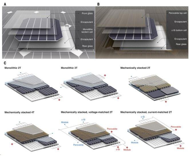
Most experimental work has focused on monolithic tandem structures with two-terminal (2T) configurations, where perovskite cells are fabricated on top of c-Si solar cells connected in series via internal junctions (Fig. 1A). Although monolithic cells require fewer transparent electrodes, BOM, and BOS components than other tandem configurations, their optimal performance requires current matching, which requires tuning the bandgap of the top cell through compositional engineering of the perovskite . When a third terminal is introduced, such as using a c-Si bottom cell with a crossed back electrode, the need for bandgap adjustment is eliminated. However, this strategy introduces increased complexity in terms of processing and interconnection.
Series structures can also be built by mechanical stacking of subcells. In this case, the sub-cells are manufactured independently, which provides greater flexibility in processing but also increases cost. More transparent electrodes are required, often using transparent conductive oxides (TCOs), which may increase absorption losses. In addition, large perovskite subcells require multiple film patterning steps (Figure 1B), typically achieved by laser scribing. Finally, electrical isolation of the perovskite and c-Si subcells is required through appropriately chosen cell laminate materials (Figure 1C).
Figure 1 Perovskite/silicon tandem cell connection scheme
The current certified photoelectric conversion efficiency (PCE) reported for the monolithic 2T series structure is 33.9%. Overall, for mechanically stacked tandem structures, perovskite subcells can be integrated with minimal adjustments to commercial c-Si cell fabrication, which is expected to accelerate their entry into the mainstream photovoltaic market.
Point 2: Layer-by-layer analysis of devices
Silicon-based battery selection
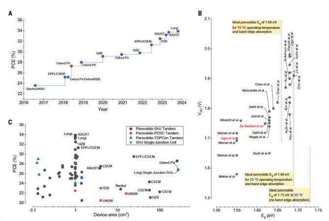
Silicon heterojunction (SHJ) solar cells with a double-sided contact layout (electrons and holes are collected on opposite sides of the cell) have been the preferred choice for building monolithic perovskite/silicon tandems, including the most recent record-breaking tandems to date. The attraction of SHJ technology lies in its high operating voltage (driven by passivated contacts, efficient light-harvesting properties, intrinsic bifacial nature, and a fabrication process that can easily achieve pin or nip series configurations. Figure 2A plots the silicon heterogeneous-based Monolithic perovskite/silicon tandem cells with junction (SHJ) bottom cells.
Figure 2C summarizes notable examples of monolithic perovskite/silicon tandem devices with large unit areas as well as laboratory-scale examples. In 2023, Oxford PV achieved a cell with 28.6% PCE for a commercial-sized tandem (258.15 cm2), likely using SHJ bottom cells, surpassing the record for single-junction c-Si cells (Longi’s 26.81%). On the other hand, Hanwha Q-Cells announced the adoption of non-SHJ substrate cell technology in its planned perovskite/silicon tandem pilot line, and JinkoSolar announced the adoption of 32.33% tandem cells on n-type TOPCon cells, indicating that The titanite/silicon tandem is technology agnostic in terms of suitable underlying cells.
Figure 2 Performance trends of perovskite/silicon tandem solar cells
Perovskite deposition technology
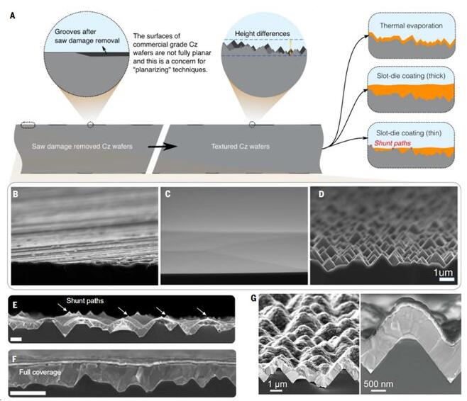
Almost all industrial single-junction c-Si cells are made from single-crystal silicon wafers, resulting in a grooved, defective surface (Figure 3A). Through alkaline wet chemical etching, the sawing damage is removed, and the surface is then textured to reduce reflection losses and promote better internal capture of weakly absorbed photons in the infrared response of the solar cell. The scanning electron microscopy (SEM) images in Figure 3B-D show a wavy surface morphology with a random pyramidal texture superimposed on it. While laboratory-grade tandem cells typically use front-side polished c-Si wafers because this makes processing the top cell easier, industrial tandem cells may require the use of double-sided textured wafers due to their optical advantages and the expensive cost of wafer polishing. For tandem cells using solution-processed perovskites, perovskites that are too thin can form shunt paths through exposed pyramids (Figure 3E); perovskites that are too thick can lead to poor carrier collection. In contrast, conformal coating technology is not limited by texture size (Figure 3G).
Figure 3 Surface morphology of industrial silicon wafer
Spin-coating of perovskite precursors combined with antisolvent treatment for thin-film crystallization and additive engineering for defect passivation has resulted in the highest-performing perovskite single-junction and perovskite/silicon tandem solar cells. However, material waste and limited scalability and throughput undermine the commercial prospects of this manufacturing route. These limitations can be overcome by slot-die coating, however, several challenges related to slot-die coating have emerged, which may explain the lack of large-scale demonstrations to date. Physical vapor deposition techniques, such as thermal evaporation, can produce directional material transfer, which is attractive for scalable conformal coatings on textured surfaces with precise film thickness control. But even for single-junction PSCs, fully evaporated perovskites have rarely been reported, perhaps in part because of the high capital expenditure and low throughput of lab-scale tools. Overall, linear evaporation, slit-chip coating, or their combination in a hybrid approach may be the most promising candidates for monolithic tandem scaling of perovskite deposition. However, in the absence of a well-established scaling platform, alternative technologies also deserve deeper exploration, such as pulsed laser deposition (PLD) or even magnetron sputtering – both of which can transfer stoichiometric material from the target to The substrate undergoes perovskite deposition.
Reducing electrical shunting in perovskite subcells
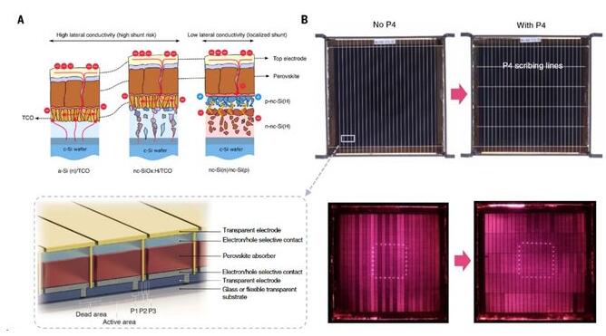
During perovskite processing, defects that enhance recombination may form, reducing the voltage of the device. Voids and cracks as well as compositional inhomogeneities can lead to undesirable localized shunts inside the perovskite cell. These defects can arise from substrate morphology, surface energy, and coating-related inhomogeneities. Resulting in PCE losses in industrial-sized perovskite photovoltaic cells. This effect, shown in Figure 2C, will be particularly pronounced for monolithic tandem structures that need to be scaled to industrial c-Si wafer sizes (>100 cm2). The effects of local shunting can be reduced by structures based on doped nanocrystalline silicon (nc-Si) films (Figure 4A) or thinner and more resistive TCOs.
Figure 4 Electrical shunting in series solar cells
For a mechanically stacked tandem structure, the perovskite top cell would cover a size as large as its coating glass (>1 m2). To pattern the perovskite top cell and reduce resistive losses at the cell level, several laser scribing steps are required (usually three, in a specific processing sequence called P1, P2, and P3). These steps divide the cells into smaller units and connect adjacent cells in series, as shown in Figure 4B. This separation also reduces the impact of local shunts on overall cell performance. An additional fourth scribe line (P4) is used to subdivide the cell to isolate areas of poorer performance. The benefits of this approach are visible through the overall improved electroluminescence (EL) response of the cell, manifested by reduced dark areas (meaning low EL emission and therefore poor photovoltaic performance) and increased pink areas (meaning high EL emission and high photovoltaic performance) (Figure 4B). An alternative strategy to reduce the impact of defects might lie in preparing smaller sized perovskite subcell coupons and then integrating them into a tandem structure at the cell lamination level. Despite these mitigation strategies, developing large-scale, leakage-free perovskite films is critical for reproducible large-scale perovskite fabrication.
Point 3: Power generation and component reliability
Perovskite band gap regulation
Initially, the monolithic tandem structure employed CH3NH3PbI3, an early halide perovskite with a band gap of about 1.55 eV. Mixed iodine-bromine perovskites can produce a band gap of approximately 1.73 eV, which is an ideal value for a single-sided monolithic tandem structure based on theoretical PCE limit calculations. However, perovskites with band gaps larger than 1.68 eV often suffer from light-induced phase separation, which remains an unsolved challenge. In addition, deviations from the standard test conditions (STC) (25°C, 1sun, AM1.5G) occurring in actual outdoor environments, such as temperature and spectral changes, can affect the current generation of each sub-cell in the series cell; device level Spectrum-dependent optical losses such as reflection and parasitic absorption may have similar effects.
The ideal perovskite band gap that maximizes power output will depend on these deviations (Figure 2B). For example, in sunny climates, the actual operating temperature of the battery can be as high as 60°C. Under such conditions, the band gaps of perovskite and silicon are affected by temperature broadening and narrowing respectively, making the ideal perovskite band gap of a single-sided monolithic series connection less than 1.68 eV. Therefore, the expected geographic location of operations may become an additional parameter to consider when designing commercial tandems.
LCOE and stability
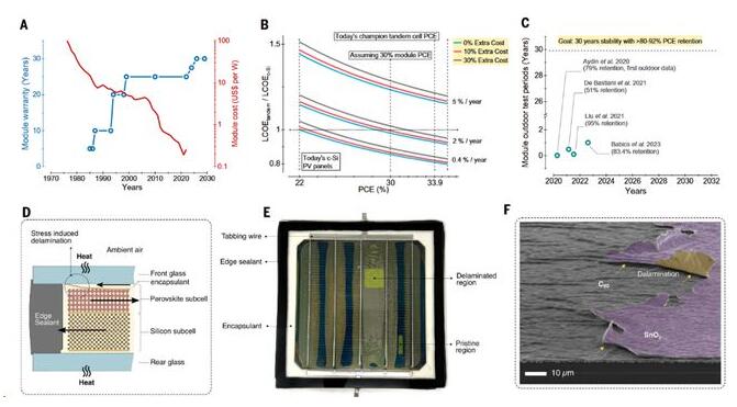
To be commercially competitive, perovskite/silicon tandem cells should have warranties comparable to mainstream c-Si-based cells, which are currently typically 25 years, although some manufacturers already offer warranties of up to 40 years ( Figure 5A). A simple LCOE calculation by considering a lifetime of 25 years reveals an acceptable annual degradation rate for a perovskite/silicon tandem structure. For reference, a 22% PCE c-Si cell was used with a relative annual degradation rate of 0.4% for LCOE calculations, which represents the commercial state of the art (maintaining >90% relative PCE over 25 years). Then, the higher annual degradation rate was considered and combined with different variable component costs (0%, 10% and 30%) to compare the LCOE of the tandem structure with c-Si cells (Figure 5B). If a similar annual degradation rate (0.4% relative) can be guaranteed, and assuming only a 30% additional cost due to perovskite subcell processing, the tandem cell should have >24% PCE to compete with mainstream c-Si PV . Under similar cost assumptions, if the annual degradation rate is 2%, a tandem cell PCE of >32% is required to be competitive. Taking into account the inevitable cell-to-cell losses, the required series cell PCE will need to be higher. To date, based on outdoor data, the maximum annual degradation rate of perovskite/silicon tandem structures of small area (1 cm2, initial PCE of packaged cells is 21.4%) is greater than 17%, which data value emphasizes the improvement of perovskite/silicon tandem structures. urgency for the stability of silicon tandem solar cells.
Figure 5 Reliability and LCOE of perovskite/silicon tandem modules
Outdoor testing of perovskite/silicon tandem cells provides valuable insights into practical stability issues that may arise during field operation while covering all aspects of degradation such as heat, light, humidity, temperature cycling, and voltage bias . Preliminary tests have identified ion migration and phase decomposition in perovskites as major issues to be aware of. Substantial progress has been made in solving key stability issues (hygrothermal and maximum power point tracking at high temperatures) for FAPbI3-based low-bandgap (~1.55 eV) cells. However, the use of wide-bandgap perovskites (~1.67 to 1.70 eV) in perovskite/silicon tandems with mixed halide (iodide, bromide, and chloride) compositions remains a more complex challenge.
Battery reliability and life prediction
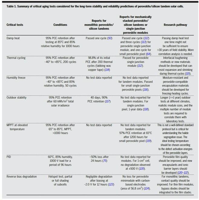
To determine the durability of perovskite/silicon tandem assemblies, accelerated tests that can give predictions in shorter times are needed. Crystalline silicon PV manufacturers have established protocols that can effectively predict potential early failures that may occur during field operations. For example, the IEC 61215 protocol includes a series of controlled laboratory accelerated degradation tests such as moist heat, thermal cycling, humidity freezing, ultraviolet (UV) exposure, and potential-induced degradation (PID) testing. Confidence in this agreement is based on statistical feedback from reported long-term outdoor test data, with perovskite/silicon tandem data still scarce (Figure 5C). Table 1 provides an overview of the aging schemes proposed so far for perovskite cells. Correlation analysis between these laboratory tests and field performance can be used to evaluate how long these devices, particularly perovskite subcells, can remain operational under field conditions.
Battery packaging
Mainstream c-Si cell packaging consists of vacuum lamination of cell strings between a front glass plate and a rear polymer backsheet with two layers of encapsulant. The porosity of typical polymer backsheets makes them unsuitable for perovskite-based photovoltaics because moisture can get in—water can quickly degrade perovskite devices. Instead, the polymer backplate needs to be replaced with a second glass plate, and the cell edges need to be sealed with rubber (Figure 5D). In this case, the initial degradation products of the perovskite absorber are iodine gas, methyl iodide, and hydriodic acid. In addition, typical mainstream photovoltaic encapsulants, such as ethylene vinyl acetate copolymer (EVA), polyolefin elastomer (POE), EVA/POE/EVA, and thermoplastic polyurethane (TPU), require a mild vacuum of 120 to 140°C. for 15 min, however temperatures >110°C are often sufficient to induce degradation of the perovskite, organic interlayer, and their interface.
Furthermore, fullerene (C60) used as the electron transport layer (ETL) in perovskite top cells is only weakly bonded to adjacent layers due to thermal expansion coefficient mismatch during the lamination process and temperature cycling. The resulting force is prone to fracture and peeling (Figure 5E). Figure 5F shows an example of the perovskite top cell in the tandem structure experiencing peeling at its C60/SnO2 interface, where SnO2 is widely used as a buffer layer to prevent sputter damage during the deposition of the top TCO. This problem may be mitigated by functionalizing C60 and using encapsulation materials with low elastic modulus. Therefore, developing new encapsulation materials with lower water vapor transmission rate and higher volume resistivity may be a necessary means to further improve the long-term stability of perovskite/silicon tandem cells. Finally, appropriate encapsulation materials may enhance the resistance of perovskite cells to PID.
Point 4: Emerging concepts
Double sided series connection
Bifacial solar cells have transparent rear contacts to take advantage of diffuse and reflected light from the environment and the ground (known as albedo) to increase their current output by a relative 10% to 30%, depending on the specific deployment. Bifacial silicon modules are rapidly becoming a dominant technology at utility scale. Calculations show that the energy yield of perovskite/silicon tandems can also be increased using the bifacial concept. This calculation requires accurate knowledge of front and rear irradiance, as well as potential (non-uniform and temporal) shadowing of the surrounding environment.
Triple junction and all-perovskite tandem
For double-junction perovskite/silicon tandem solar cells, over 37% PCE can be achieved (the theoretical limit is about 44%). Higher practical values are undoubtedly possible for triple-junction perovskite/perovskite/silicon tandem solar cells, with a theoretical limit of 49.4%. In the monolithic triple structure, current matching is again required, which requires a band gap of about 1.45 eV in the middle cell, which can be achieved by a mixed-metal lead-tin perovskite composition with a relatively high tin content. However, tin-based perovskites are susceptible to oxidation-induced degradation. For the top cell, a bandgap of approximately 1.95 eV is required and a mixed halide perovskite composition with a relatively high bromine content can be used. However, these perovskites undergo light-induced phase separation and lead to higher Voc depletion at the device level. Inorganic perovskites may avoid phase separation but need to be prepared at relatively low temperatures (around 100°C) for monolithic integration.
Another obstacle to triple-junction tandem structures stems from the need to prepare perovskite subcells on top of other perovskite subcells, which may lead to compatibility with similar processing encountered when scaling up double-junction perovskite/perovskite tandem cells. Sexual challenges. Fortunately, advances made in perovskite/perovskite tandem cells can be adapted to triple-junction tandem cells. If existing limitations of medium- and wide-bandgap perovskites can be addressed, it may even become attractive to develop efficient and stable perovskite formulations with bandgaps close to c-Si (1.12 eV) to build all-Ca Titanium tandem structure. Such materials would open a path to eliminating c-Si from devices. Achieving efficient and stable tin-based perovskites is crucial for this and has been a long-standing challenge.
Key Point 5: Sustainability in Manufacturing
The main challenges for the industrialization of perovskite/silicon solar tandems are related to scale performance, reliability and capital expenditure. However, the raw material costs and sustainability involved, as well as operational expenditure (OpEx), are also critical to scale manufacturing. For example, all battery configurations require at least one TCO, and indium-based TCOs have desirable properties such as high transparency, conductivity, and durability. Although recent research claims that indium production could meet solar cell demand under certain scenarios, it is crucial to remain vigilant about potential supply risk issues that could arise from indium scarcity. Minimizing the thickness and number of TCOs required in the device, where 2T doublets have the advantage, can reduce these risks.
Lead leakage from components and the use of harmful solvents during the manufacturing process are two major issues with perovskite tandem PV, but these issues can be mitigated through component inspection and replacement before catastrophic failure. Recent research suggests that the environmental impact of battery failure will only be moderate. Solution-processed perovskites should go through waste management, purification, and recycling processes to mitigate solvent-induced toxicity issues. Alternatively, green solvents and vacuum deposition methods can be considered while retaining the properties of the perovskite layer.
4. Market Current Situation: Challenges and Opportunities Coexist
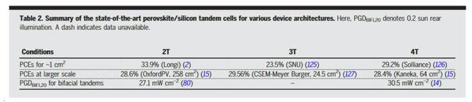
It is expected that by 2032, tandem photovoltaic technology will account for more than US$10 billion in market share. However, predicting the realistic date for perovskite/silicon tandems to successfully enter the market remains challenging, and Table 2 summarizes the highest perovskite/silicon tandem PCEs at different scales.
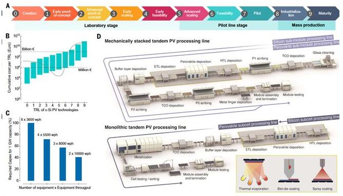
In any case, the technology must successfully pass various Technology Readiness Levels (TRLs) before it can be commercialized, including laboratory studies (TRL1-5), pilot lines (TRL5-8), and volume production (TRL8,9) , as shown in Figure 6A. Over the years, the photovoltaic industry has accumulated considerable knowledge and expertise in thin film and silicon technologies, which requires extensive and expensive R&D efforts over several years, as shown in Figure 6B. Much of this can be accommodated within the time and budget requirements of perovskite/silicon tandem technology. However, substantial and sustained funding is critical for its successful commercialization. Currently, an R&D laboratory focused on perovskite subcell (or subcell) development can be set up with a budget of less than ~5 million euros.
Figure 6 Industrialization of perovskite/silicon tandems
One of the key drivers of c-Si photovoltaic production cost reductions is the significant increase in throughput, with c-Si processing steps reaching production rates of over 10,000 wafers per hour. Perovskite/silicon tandems require similar processing throughput to achieve competitive LCOE values. Figure 6C illustrates that increasing the throughput of a physical vapor deposition line by approximately three times can reduce capital expenditures by >50%, thereby lowering the levelized cost of electricity. In Figure 6D, conceptual processing lines for mechanical stacking and monolithic series cells are depicted. Mechanically stacked tandems require additional processing steps for perovskite subcells, including multiple laser scribing, and they require complex cell assembly lines, which results in increased overall capital expenditures. On the other hand, the packaging procedure for monolithic cells is similar to that of c-Si single-junction modules, requiring only wafer-level processing steps for the perovskite subcells. A recent techno-economic analysis confirmed that mechanically stacked tandems can be more expensive to produce than monolithic tandems.
Additional challenges have arisen in characterizing industrially produced perovskite/silicon tandem technologies. Current-voltage (IV) analysis under millisecond-scale illumination is commonly used for industrial characterization of c-Si cells. New methods must be developed to quickly and reliably measure perovskite/silicon tandems.
5. References
Erkan Aydin et al. Pathways toward commercial perovskite/silicon tandem photovoltaics , Science
Doi: 10.1126/science.adh3849 (2024).
 E-mail: info@chemborun.com
 Tel: +86-574-87178138
  No. 1558, Jiangnan Road,, Ningbo, Zhejiang, China (Mainland)/31