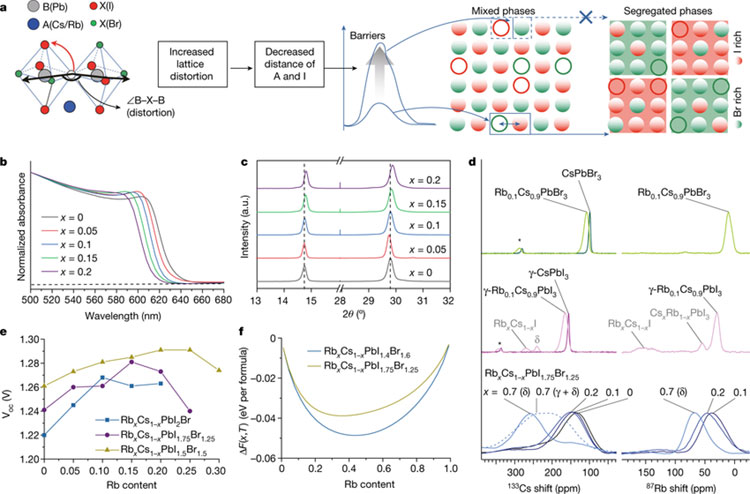
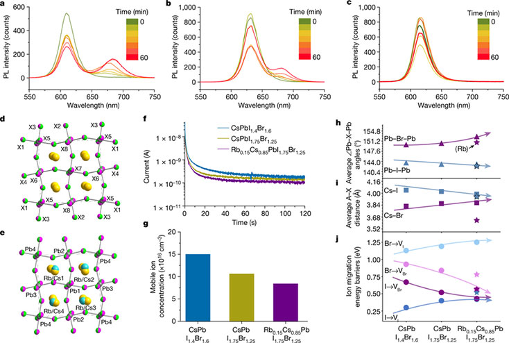
The phenomena and mechanism of suppressed LIPS a–c, PL spectra of CsPbI1.4Br1.6 (a), CsPbI1.75Br1.25 (b) and Rb0.15Cs0.85PbI1.75Br1.25 (c) perovskite films under 1-sun AM 1.5G illumination for 60 min. d,e, The structures of the crystals from the loading compositions CsPbI1.4Br1.6 and CsPbI1.75Br1.25 (d) and Rb0.15Cs0.85PbI1.75Br1.25 (e) as viewed down the crystallographic b axis. The halide positions are labelled by X (where X is I or Br), and the labelling scheme for the atoms is consistent between the two structures. The Rb, Cs, Pb, I and Br atoms are labelled in blue, yellow, grey, pink and green, respectively. The fractional occupancy of the halide sites is shown as partially filled sectors. Halide sites X1–X4 propagate in the a–c plane, and halide sites X5–X8 propagate down the b axis. f,g, Transient ion-migration currents (f) and calculated mobile ion concentrations (g) of CsPbI1.4Br1.6, CsPbI1.75Br1.25 and Rb0.15Cs0.85PbI1.75Br1.25 PSCs. h–j, DFT-calculated average ∠Pb–Χ–Pb (where X is I or Br) (h), average A···X interatomic distance (i) and ion-migration energy barrier of I (or Br) to VI (or VBr) (j) for CsPbI1.4Br1.6, CsPbI1.75Br1.25 and Rb0.15Cs0.85PbI1.75Br1.25. The arrows represent their trends. For Rb0.15Cs0.85PbI1.75Br1.25, the information around the Rb atoms is labelled with stars. Owing to the supercell limitations, the real compositions used in calculations are CsPbI1.375Br1.625 (for CsPbI1.4Br1.6), CsPbI1.75Br1.25 (for CsPbI1.75Br1.25) and Rb0.125Cs0.875PbI1.75Br1.25 (for Rb0.15Cs0.85PbI1.75Br1.25).
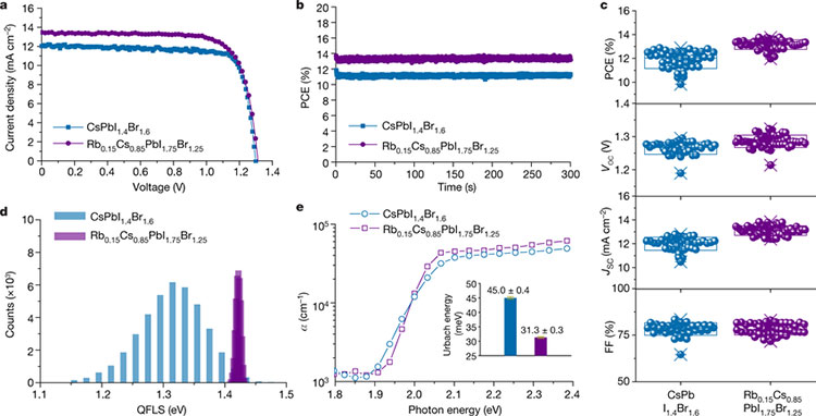
PV performance of 2.0-eV single-junction PSCs a,b, J–V curves (a) and SPO (b) of approximately 2.0-eV CsPbI1.4Br1.6 and Rb0.15Cs0.85PbI1.75Br1.25 PSCs. c, Statistics of PCE, VOC, JSC and FF of the CsPbI1.4Br1.6 devices (41 samples) and the Rb0.15Cs0.85PbI1.75Br1.25 devices (54 samples). d, Histogram of QFLS pixel values of CsPbI1.4Br1.6 and Rb0.15Cs0.85PbI1.75Br1.25 perovskites taken from larger 100 µm × 100 µm images. e, Near-bandgap absorption coefficient (α) spectra from PDS for CsPbI1.4Br1.6 and Rb0.15Cs0.85PbI1.75Br1.25 thin films. Inset: Urbach energy extracted from the PDS measurements.
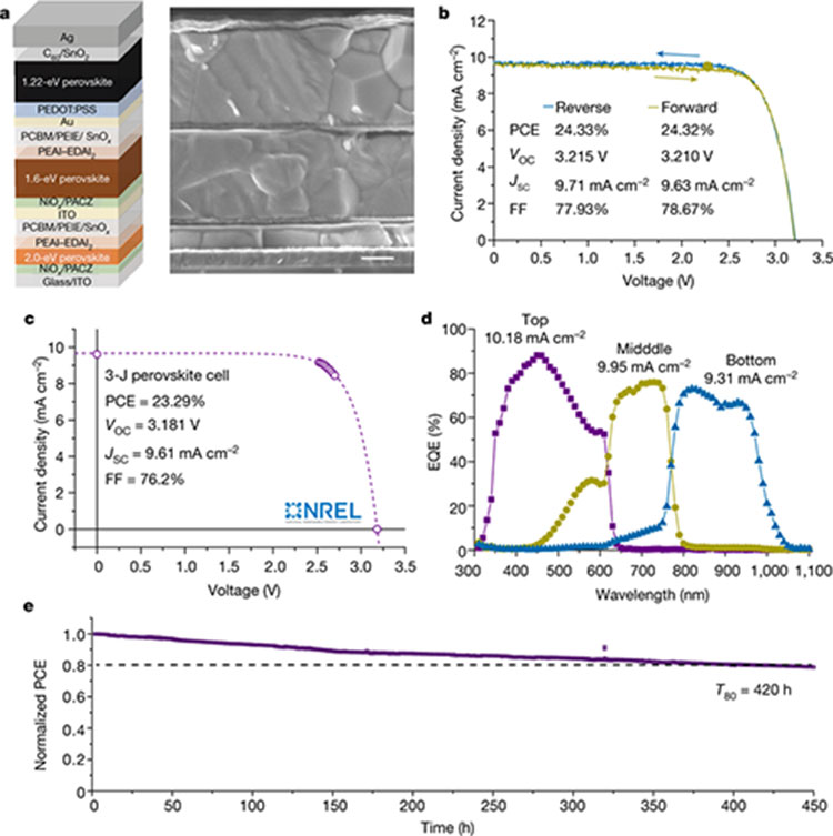
PV performance and stability of all-perovskite TJSCs a, Schematic diagram of device structure and corresponding cross-sectional scanning electron microscopy image of the all-perovskite TJSC. Scale bar, 400 nm. b, J–V curves of reverse and forward scans for a champion all-perovskite TJSC. The J–V performances of the single-junction cells in all-perovskite triple-junction solar cells based on Ag electrodes are shown in Supplementary Table 10. c, NREL-certified quasi-steady-state J–V curve of the all-perovskite triple-junction device. d, EQE curves of the approximately 2.0-eV, approximately 1.6-eV and approximately 1.22-eV subcells within the TJSC. e, The maximum-power-point stability tracking of an encapsulated TJSC at room temperature under simulated AM 1.5G 1-sun illumination. T80 is the time taken for device efficiency to reduce to 80% of its initial value.
all-perovskite TJSC. The configuration of the TJSC is ITO glass / NiOx / Me-4PACz / 2.0-eV inorganic perovskite (170 nm) / PEAI –EDAI2 / PCBM / PEIE / SnOx / ITO / NiOx / Me-4PACz / 1.6-eV perovskite (780 nm) / PEAIEDAI2 / PCBM / PEIE / SnOx / gold (Au) / poly (3,4-ethylenedioxythiophene ) polystyrene sulfonate (PEDOT:PSS ) / 1.22-eV SnPb perovskite (870 nm )/ C60 / SnOx / Ag (Fig. 4a). Figure 4b shows the J–V curves of a champion
all-perovskite TJSC. The PCE from the reverse scan is 24.33% with a VOC of 3.215 V, a short-circuit current ( JSC) of 9.71 mA cm−2 and a fill factor (FF) of 77.93%. There is negligible hysteresis between the forward and reverse J–V scans of the device (Fig. 4b). We achieved a certified quasi-steady-state PCE of 23.29% in an accredited independent PV calibration laboratory (National Renewable Energy Laboratory (NREL);
Fig. 4c and Supplementary Fig. 22), which is, to our knowledge, the first
reported certified PCE for perovskite-based TJSCs. The SPO efficiency
over 20 min is 24.1% (Supplementary Fig. 23). The integrated JSC values
for the approximately 2.0-eV, approximately 1.6-eV and approximately
1.22-eV cells from external quantum efficiency (EQE) measurements of
a TJSC are 10.18 mA cm−2, 9.95 mA cm−2 and 9.31 mA cm−2, respectively
(Fig. 4d). The J–V performance from 32 devices is detailed in Supplementary Fig. 24. The efficiency of all-perovskite TJSCs will further improve
through the development of new passivation strategies, improved
interfacial contact and the optimization of light management (Supplementary Table 11 and Supplementary Note 11 for a detailed discussion).
We tracked the PCE of an encapsulated device stored in a nitrogen
glovebox. After 120 days, the PCE shows a negligible decline (Supplementary Fig. 23). We also monitored the performance of an encapsulated TJSC under maximum-power-point tracking conditions and
continuous AM 1.5G 1-sun illumination at room temperature in an
ambient atmosphere (Fig. 4e). The optimized device based on a Rb/Cs
mixed-cation perovskite retains 80% of its initial PCE after 420 h of continuous operation. Further analysis shows that 2.0-eV Rb/Cs perovskites undergo phase segregation after 450 h of maximum-power-point
tracking (Supplementary Fig. 25, Supplementary Table 12 and Supplementary Note 12 for a detailed discussion). These results indicate
that, although Rb incorporation offers a promising route to decreased
light-induced phase segregation, the topic will benefit from further
study along the path to a long-term operating lifetime solution.
Online content
Any methods, additional references, Nature Portfolio reporting summaries, source data, extended data, supplementary information, acknowledgements, peer review information; details of author contributions
and competing interests; and statements of data and code availability
are available at https://doi.org/10.1038/s41586-023-06006-7 .
1. Stoumpos, C. C., Malliakas, C. D. & Kanatzidis, M. G. Semiconducting tin and lead iodide perovskites with organic cations: phase transitions, high mobilities, and near-infrared photoluminescent properties. Inorg. Chem. 52, 9019–9038 (2013).
2. Eperon, G. E., Hörantner, M. T. & Snaith, H. J. Metal halide perovskite tandem and multiple-junction photovoltaics. Nat. Rev. Chem. 1, 0095 (2017).
3. Hoke, E. T. et al. Reversible photo-induced trap formation in mixed-halide hybrid perovskites for photovoltaics. Chem. Sci. 6, 613–617 (2015).
4. McMeekin, D. P. et al. A mixed-cation lead mixed-halide perovskite absorber for tandem solar cells. Science 351, 151–155 (2016).
5. Abdi-Jalebi, M. et al. Maximizing and stabilizing luminescence from halide perovskites with potassium passivation. Nature 555, 497–501 (2018).
6. Xiao, K. et al. Solution-processed monolithic all-perovskite triple-junction solar cells with efficiency exceeding 20%. ACS Energy Lett. 5, 2819–2826 (2020).
7. Henry, C. H. Limiting efficiencies of ideal single and multiple energy gap terrestrial solar cells. J. Appl. Phys. 51, 4494–4500 (1980).
8. Shockley, W. & Queisser, H. J. Detailed balance limit of efficiency of p‐n junction solar cells. J. Appl. Phys. 32, 510–519 (1961).
9. Pazos-Outon, L. M. et al. Photon recycling in lead iodide perovskite solar cells. Science 351, 1430–1433 (2016).
10. Best research-cell efficiencies. NREL https://www.nrel.gov/pv/cell-efficiency.html (2022).
11. Green, M. A. et al. Solar cell efficiency tables (version 60). Prog. Photovolt. Res. Appl. 30, 687–701 (2022).
12. Kojima, A., Teshima, K., Shirai, Y. & Miyasaka, T. Organometal halide perovskites as visible-light sensitizers for photovoltaic cells. J. Am. Chem. Soc. 131, 6050–6051 (2009).
13. Lee, M. M., Teuscher, J., Miyasaka, T., Murakami, T. N. & Snaith, H. J. Efficient hybrid solar cells based on meso-superstructured organometal halide perovskites. Science 338, 643–647 (2012).
14. Kim, H. S. et al. Lead iodide perovskite sensitized all-solid-state submicron thin film mesoscopic solar cell with efficiency exceeding 9%. Sci. Rep. 2, 591 (2012).
15. Xu, J. et al. Triple-halide wide-band gap perovskites with suppressed phase segregation for efficient tandems. Science 367, 1097–1104 (2020).
16. Hörantner, M. T. et al. The potential of multijunction perovskite solar cells. ACS Energy Lett. 2, 2506–2513 (2017).
17. McMeekin, D. P. et al. Solution-processed all-perovskite multi-junction solar cells. Joule 3, 387–401 (2019).
18. Wang, J. et al. 16.8% monolithic all-perovskite triple-junction solar cells via a universal two-step solution process. Nat. Commun. 11, 5254 (2020).
19. Zheng, J. et al. Monolithic perovskite–perovskite–silicon triple-junction tandem solar cell with an efficiency of over 20%. ACS Energy Lett. 7, 3003–3005 (2022).
20. Muscarella, L. A. et al. Lattice compression increases the activation barrier for phase segregation in mixed-halide perovskites. ACS Energy Lett. 5, 3152–3158 (2020).
21. Rehman, W. et al. Photovoltaic mixed-cation lead mixed-halide perovskites: links between crystallinity, photo-stability and electronic properties. Energy Environ. Sci. 10, 361–369 (2017).
22. Beal, R. E. et al. Cesium lead halide perovskites with improved stability for tandem solar cells. J. Phys. Chem. Lett. 7, 746–751 (2016).
23. Brennan, M. C., Draguta, S., Kamat, P. V. & Kuno, M. Light-induced anion phase segregation in mixed halide perovskites. ACS Energy Lett. 3, 204–213 (2017).
24. Noh, J. H., Im, S. H., Heo, J. H., Mandal, T. N. & Seok, S. I. Chemical management for colorful, efficient, and stable inorganic-organic hybrid nanostructured solar cells. Nano Lett. 13, 1764–1769 (2013).
25. Yuan, Y. B. & Huang, J. S. Ion migration in organometal trihalide perovskite and its impact on photovoltaic efficiency and stability. Acc. Chem. Res. 49, 286–293 (2016).
26. Beal, R. E. et al. Structural origins of light-induced phase segregation in organic– inorganic halide perovskite photovoltaic materials. Matter 2, 207–219 (2020).
27. Marronnier, A. et al. Anharmonicity and disorder in the black phases of cesium lead iodide used for stable inorganic perovskite solar cells. ACS Nano 12, 3477–3486 (2018).
28. Zhou, W. et al. Light-independent ionic transport in inorganic perovskite and ultrastable Cs-based perovskite solar cells. J. Phys. Chem. Lett. 8, 4122–4128 (2017).
29. Kubicki, D. J., Stranks, S. D., Grey, C. P. & Emsley, L. NMR spectroscopy probes microstructure, dynamics and doping of metal halide perovskites. Nat. Rev. Chem. 5, 624–645 (2021).
30. Kubicki, D. J. et al. Phase segregation in Cs-, Rb- and K-doped mixed-cation (MA)x(FA)1−xPbI3 hybrid perovskites from solid-state NMR. J. Am. Chem. Soc. 139, 14173–14180 (2017).
31. Xiao, J. W. et al. Stabilizing RbPbBr3 perovskite nanocrystals through Cs+ substitution. Chem. Eur. J. 25, 2597–2603 (2019).
32. Stoumpos, C. C. & Kanatzidis, M. G. The renaissance of halide perovskites and their evolution as emerging semiconductors. Acc. Chem. Res. 48, 2791–2802 (2015).
33. Linaburg, M. R., McClure, E. T., Majher, J. D. & Woodward, P. M. Cs1−xRbxPbCl3 and Cs1−xRbxPbBr3 solid solutions: understanding octahedral tilting in lead halide perovskites. Chem. Mater. 29, 3507–3514 (2017).
34. Deng, Y. et al. Defect compensation in formamidinium–caesium perovskites for highly efficient solar mini-modules with improved photostability. Nat. Energy 6, 633–641 (2021).
35. Eames, C. et al. Ionic transport in hybrid lead iodide perovskite solar cells. Nat. Commun. 6, 7497 (2015).
36. El-Hajje, G. et al. Quantification of spatial inhomogeneity in perovskite solar cells by hyperspectral luminescence imaging. Energy Environ. Sci. 9, 2286–2294 (2016).
37. Subedi, B. et al. Urbach energy and open-circuit voltage deficit for mixed anion–cation perovskite solar cells. ACS Appl. Mater. Interfaces 14, 7796–7804 (2022).
38. Mahesh, S. et al. Revealing the origin of voltage loss in mixed-halide perovskite solar cells. Energy Environ. Sci. 13, 258–267 (2020).
Publisher’s note Springer Nature remains neutral with regard to jurisdictional claims in published maps and institutional affiliations.
Springer Nature or its licensor (e.g. a society or other partner) holds exclusive rights to this article under a publishing agreement with the author(s) or other rightsholder(s); author self-archiving of the accepted manuscript version of this article is solely governed by the terms of such publishing agreement and applicable law.
Materials
All materials were used as received without further purification. Lead iodide (PbI2, 99.99%), lead bromide (PbBr2, 99.999%) and Me-4PACz were purchased from TCI chemicals. Caesium iodide (CsI, 99.999%), caesium bromide (CsBr, >99.9%), rubidium bromide (RbBr, 99.6%), tin(II) iodide (SnI2, 99.99%, Beads), tin(II) fluoride (SnF2, 99%), glycine hydrochloride (99%), guanidine thiocyanate (GuaSCN, 99%), EDAI2 (98%), polyethyleneimine, 80% ethoxylated solution (PEIE, 37 wt% in water), nickel(II) nitrate hexahydrate (Ni(NO3)2·6H2O, 99.999%) and sodium hydroxide (NaOH, ≥99.99%) were purchased from Sigma-Aldrich. Methylammonium iodide (MAI), formamidinium iodide (FAI), formamidinium chloride (FACl) and PEAI were purchased from GreatCell Solar Materials. PCBM (99.5%) and C60 were purchased from Nano-C. Tetrakis(dimethylamino) tin(IV) (99.99%-Sn, 50–1815 Tin) was purchased from Strem Chemicals. Dimethyl sulfoxide (DMSO, 99.9%), N,N-dimethylformamide (DMF, 99.8%), 2-propanol (IPA, 99.5%), chlorobenzene (CB, 99.8%), anisole (99.7%) and 1-propanol (99.7%) were purchased from Sigma-Aldrich. Toluene (99.8%) was purchased from Alfa Aesar. PEDOT:PSS aqueous solution (Al-4083) was purchased from Ossila. Commercial ITO substrates (20 Ω sq−1) with 25 mm × 25 mm dimension were purchased from TFD. Quartz substrates were purchased from Shenzhen Weina Technology Electronic. Preparation of inorganic perovskite precursor solutions The precursor chemicals were mixed stoichiometrically with anhydrous dimethyl sulfoxide solvent and stirred until completely dissolved. Before use, the perovskite precursor solution was filtered through a 0.22-µm polytetrafluoroethylene (PTFE) membrane.
FACl (FACl:Pb2+ = 0.1 mmol:1 mmol) was added into the I/Br mixed precursor solutions as an additive to improve the interfacial contact of inorganic perovskite and substrate39. FACl was evaporated during the annealing process at 180 °C (Supplementary Fig. 9)40. For simplicity, we do not show the 0.1 mmol FACl additive and 1 ml DMSO in the following recipes.
1 M Rb0.15Cs0.85PbI1.75Br1.25 = 0.15 mmol RbI + 0.85 mmol CsI + 0.375 mmol PbI2 + 0.625 mmol PbBr2
1 M CsPbI1.4Br1.6 = 1 mmol CsI + 0.2 mmol PbI2 + 0.8 mmol PbBr2
1 M CsPbI1.75Br1.25 = 1 mmol CsI + 0.375 mmol PbI2 + 0.625 mmol PbBr2
1 M RbPbI1.75Br1.25 = 1 mmol RbI + 0.375 mmol PbI2 + 0.625 mmol PbBr2
1 M CsPbI2Br = 1 mmol CsI + 0. 5 mmol PbI2 + 0.5 mmol PbBr2
1 M RbPbI2Br = 1 mmol RbI + 0. 5 mmol PbI2 + 0.5 mmol PbBr2
1 M CsPbI1.5Br1.5 = 1 mmol CsI + 0. 25 mmol PbI2 + 0.75 mmol PbBr2
1 M RbPbI1.5Br1.5 = 1 mmol RbI + 0. 25 mmol PbI2 + 0.75 mmol PbBr2
For pure-Br precursor solutions, the concentration was 0.5 M without
additives because 1 M cannot be dissolved in DMSO.
0.5 M CsPbBr3 = 0.5 mmol CsBr + 0.5 mmol PbBr2
0.5 M RbPbBr3 = 0.5 mmol RbBr + 0.5 mmol PbBr2
DMAI (DMAI:Pb2+ = 1 mmol:1 mmol) was added into the following pure-I precursor solutions as an additive to promote the formation of pure-I inorganic perovskites41. DMAI was evaporated during the annealing process at 250 °C (ref. 42). For simplicity, we do not show
the 1 mmol DMAI additive and 1 ml DMSO in the following recipes.
1 M CsPbI3 = 1 mmol CsI + 1 mmol PbI2
1 M RbPbI3 = 1 mmol RbI + 1 mmol PbI2
RbxCs1−xPbX3 (where X is I or Br) precursor solutions can be obtained by mixing the CsPbX3 and RbPbX3 precursor solutions based on volume ratios.
NiOx nanoparticle synthesis
The NiOx nanoparticles were prepared by hydrolysis of nickel nitrate following previous work43. Briefly, Ni(NO3)2·6H2O (20 mmol) was dissolved in deionized water (20 ml) to obtain a dark-green solution. Then, NaOH aqueous solution (4 ml, 10 M) was slowly added to the dark-green solution with stirring. After stirring for 20 min, the colloidal precipitate was washed thoroughly using deionized water three times and dried at 80 °C for 6 h. The obtained green powder was then calcined at 270 °C for 2 h to obtain a black powder. The NiOx nanoparticle ink was prepared by dispersing the obtained NiOx nanoparticles in a mixed solution of deionized water and IPA (3:1, v/v) for a concentration of 5 mg ml−1. Inorganic perovskite device fabrication
The configuration of inorganic perovskite devices was ITO glass/NiOx/ Me-4PACz/inorganic perovskite/PEAI–EDAI2/PCBM/PEIE/SnOx/Ag. The pre-patterned ITO glasses were sequentially sonicated in acetone and IPA each for 20 min. After drying with nitrogen, the substrates were exposed to UV-ozone treatment for 20 min to remove organic contaminants.
NiOx layers were prepared by spin-coating 100 µl NiOx nanoparticle solution on ITO substrates at 3,000 rpm for 25 s in the air without any post-treatment, then immediately transferred to a nitrogen-filled glovebox.
For the Me-4PACz layer, 100 µl Me-4PACz (0.5 mg ml−1) solution
in ethanol was spin-coated on the NiOx film at 3,000 rpm for 30 s in
a nitrogen-filled glovebox. Then the prepared film was annealed at
100 °C for 10 min.
For Br-based or I/Br mixed perovskite films, 100 µl inorganic perovskite precursor solution was spin-coated on the substrate at 3,000 rpm for 70 s. The film was firstly annealed at 40 °C until the colour of the film started to turn brown (5–20 s in our lab), then quickly moved to a
180 °C hotplate for 5-min annealing. For pure-I-based inorganic perovskite, 100 µl inorganic perovskite precursor solution was spin-coated on the substrate at 3,000 rpm for 70 s. Then the film was annealed at 250 °C for 5 min.
For the PEAI–EDAI2 modified layer, the treatment solution was prepared by dissolving 1 mg PEAI and 1 mg EDAI2 into 1 ml IPA. Then 130 µl filtered solution was spin-coated on the inorganic perovskite film at 4,000 rpm for 25 s. Then the film was annealed at 100 °C for 5 min.
For the PCBM layers, 70 µl PCBM (15 mg ml−1) solution in CB was spin-coated on the inorganic perovskite/PEAI–EDAI2 film at 1,000 rpm for 30 s.
For the PEIE layers, 100 µl PEIE (0.025 wt%) solution in IPA was spin-coated on the PCBM film at 4,000 rpm for 30 s. For the SnOx layer, the film was then transferred to the atomic layer deposition system (Picosun) to deposit 20-nm SnOx at 100 °C using precursors of tetrakis(dimethylamino) tin(IV) (99.9999%) and deionized water.
The 140-nm-thick Ag electrode was deposited by thermal evaporation.
Fabrication of all-perovskite triple-junction solar cells
The configuration of the triple-junction solar cells was ITO/NiOx/
Me-4PACz/2.0-eV inorganic perovskite (170 nm)/PEAI–EDAI2/PCBM/
PEIE/SnOx/ITO/NiOx/Me-4PACz/1.6-eV perovskite (780 nm)/PEAI–
EDAI2/PCBM/PEIE/SnOx/Au/PEDOT:PSS/1.22-eV SnPb perovskite
(870 nm)/C60/SnOx/Ag.
For the approximately 2.0-eV inorganic perovskite top cell, the fabrications of ITO glass, NiOx, Me-4PACz, PEAI–EDAI2, PCBM, PEIE and SnOx
layers were the same as inorganic perovskite single-junction devices.
The PEIE layer can increase the compatibility of SnOx, which can protect
the perovskite layer from degradation when spin-coating the following
NiOx and perovskite layers44. For the 2.0-eV inorganic perovskite layers, 100 µl 0.8 M Rb0.15Cs0.85PbI1.75Br1.25 inorganic perovskite precursor
solution was spin-coated on the substrate at 3,000 rpm for 70 s. The
film was first annealed at 40 °C for 15 s, then quickly moved to a 180 °C
hotplate for 5 min.
For the ITO layer, the top cell was then transferred to the radiofrequency magnetron sputtering system. The ITO target used in this study was a commercial grade of purity of >99.99% with a size
of 3.00″ diameter × 0.125″ thick. The target composition was In2O3/
SnO2 90/10 wt%. The process pressure was 3 mtorr at an argon flow of
18 standard cubic centimetres per minute. The average deposition rate
was about 0.24 A s−1 at 33 W power. A total ITO layer thickness of 20 nm
was deposited.
For the approximately 1.6-eV perovskite middle cell, the fabrication
procedures of the NiOx, Me-4PACz, PEAI–EDAI2, PCBM, PEIE and SnOx
layers were similar to those described above for the single-junction
inorganic perovskite devices. The only difference was that the subcell
was treated by plasma etching for 30 s to increase its surface wettability before spin-coating the NiOx nanoparticle solution. For the
1.6-eV perovskite film, the Cs0.05FA0.9MA0.05Pb(I0.9Br0.1)3 perovskite
precursor solution (1.5 M) was prepared by dissolving 0.075 mmol CsI,
0.075 mmol MABr, 1.35 mmol FAI, 0.1875 mmol PbBr2 and 1.3125 mmol
PbI2 in a mixed solvent of DMF and DMSO with a volume ratio of 4:1.
The perovskite precursor solution was filtered through a 0.22-µm
PTFE membrane before use. Then 100 µl of perovskite solution was
dropped on the substrate and spin-coated at 1,000 rpm for 10 s followed by 5,000 rpm for 30 s. Then 150 µl anisole was dropped onto the
substrate at the last 5 s of the spin-coating, resulting in the formation
of dark brown films that were then annealed on a hotplate at 100 °C
for 10 min.
A 1-nm-thick Au electrode was deposited by thermal evaporation.
For the approximately 1.22-eV SnPb perovskite bottom cell,
the PEDOT:PSS layer was prepared by spin-coating 100 µl diluted
PEDOT:PSS solution with n-propanol at a volume ratio of 1:1 on the
substrate at 4,000 rpm for 30 s and then annealing at 100 °C for
15 min in ambient air. After cooling, the substrates were immediately transferred to a nitrogen-filled glovebox to deposit perovskite
films. A 1.8 M SnPb perovskite precursor solution with a composition
of Cs0.05FA0.7MA0.25Pb0.5Sn0.5I3-0.05SnF2 was prepared by dissolving
0.09 mmol CsI, 1.26 mmol FAI, 0.45 mmol MAI, 0.9 mmol SnI2, 0.9 mmol
PbI2 and 0.09 mmol SnF2 in a 1 ml mixed solvent of DMF and DMSO with a
volume ratio of 3:1. Tin powders (5 mg), GuaSCN (4 mg), 4F-PEABr (2 mg)
and glycine hydrochloride (4 mg) were added to the precursor solution.
The precursor solution was then stirred at room temperature for 1 h.
The precursor solution was filtered using a 0.22-µm PTFE membrane
before deposition. Then 70 µl of perovskite solution was deposited on
the substrate and spin-coated with a two-step spin-coating procedure:
1,000 rpm for 10 s and 3,800 rpm for 45 s. Then 300 µl CB was dropped
onto the substrate during the second spin-coating step at the last 20 s
of the spin-coating. The substrates were then annealed at 100 °C for
10 min. Finally, 20-nm C60, 20-nm SnOx and 140-nm Ag were sequentially deposited on the top of SnPb perovskite layer by organic thermal
evaporation, atomic layer deposition and metal thermal evaporation,
respectively.
Reporting summary
Further information on research design is available in the Nature
Portfolio Reporting Summary linked to this article.
Data availability
All data are available in the paper or its Supplementary Information.
The crystallographic files (CIF) for the compounds reported in this work
can be found as depositions in the Cambridge Crystallographic Data
Centre (CCDC) based on the following deposition numbers: 2211086
(CsPbI1.46Br1.54), 2211087 (CsPbI1.73Br1.27) and 2211088 (Rb0.22Cs0.78PbI1.65
Br1.35).
Code availability
The codes and post-analysis tools for calculations are available from
the FHI-aims website: https://fhi-aims.org.
39. Zhang, J. et al. Intermediate phase enhances inorganic perovskite and metal oxide
interface for efficient photovoltaics. Joule 4, 222–234 (2020).
40. Wang, Z. et al. Additive-modulated evolution of HC(NH2)2PbI3 black polymorph for
mesoscopic perovskite solar cells. Chem. Mater. 27, 7149–7155 (2015).
41. Wang, Y. et al. Thermodynamically stabilized β-CsPbI3-based perovskite solar cells with
efficiencies >18%. Science 365, 591–595 (2019).
42. Meng, H. et al. Chemical composition and phase evolution in DMAI-derived inorganic
perovskite solar cells. ACS Energy Lett. 5, 263–270 (2019).
43. Chen, H. et al. Quantum-size-tuned heterostructures enable efficient and stable inverted
perovskite solar cells. Nat. Photon. 16, 352–358 (2022).
44. Palmstrom, A. F. et al. Enabling flexible all-perovskite tandem solar cells. Joule 3,
2193–2204 (2019).
Acknowledgements This research was made possible by a US Department of the Navy, Office of Naval Research grant (N00014-20-1-2572), and the US Department of Energy’s Office of Energy Efficiency and Renewable Energy (EERE) under the Solar Energy Technologies Office Award Number DE-EE0008753. This work was supported in part by the Ontario Research Fund-Research Excellence programme (ORF7-Ministry of Research and Innovation, Ontario Research Fund-Research Excellence Round 7). M.G.K. was supported by the Office of Naval Research (ONR) under grant N00014-20-1-2725. At King Abdullah University of Science and Technology (KAUST), this work was supported by the under award no. OSR-2020-CRG9-4350.2. This work was also supported by the Natural Sciences and Engineering Council of Canada and the Vanier Canada Graduate Scholarship. Z.W. acknowledges the Banting Postdoctoral Fellowships Program of Canada. D.J.K. acknowledges the support of the University of Warwick. The UK High-Field Solid-State NMR Facility used in this research was funded by EPSRC and BSRC (EP/T015063/1), as well as the University of Warwick, including via part funding through Birmingham Science City Advanced Materials Projects 1 and 2 supported by Advantage West Midlands (AWM) and the European Regional Development Fund (ERDF). The crystallographic experiments made use of the IMSERC Crystallography and Physical Characterization facilities at Northwestern University, which received support from the Soft and Hybrid Nanotechnology Experimental (SHyNE) Resource (NSF ECCS-2025633), and Northwestern University. The purchase of the Ag-microsource used to collect both single and powder diffraction data was supported by the Major Research Instrumentation Program for the National Science Foundation under the award CHE-1920248. This work also made use of the EPIC facility at Northwestern University’s NUANCE Center, which has received support from the SHyNE Resource (NSF CCS-2025633), the IIN and Northwestern’s MRSEC programme (NSF DMR-1720139). Computations were performed on the Niagara supercomputer at the SciNet HPC Consortium. SciNet is funded by the Canada Foundation for Innovation; the Government of Ontario; Ontario Research Fund Research Excellence; and the University of Toronto. A.B. was supported, in part, by a fellowship through the National Defense Science and Engineering Graduate (NDSEG) Fellowship Program, sponsored by the Air Force Research Laboratory (AFRL), the Office of Naval Research (ONR) and Army Research Office (ARO). We thank Tao Song for efficiency certification in NREL. Z.W. thanks Yicheng Zhao, Zhenyi Ni and Emre Yengel for discussion about LIPS. A.B. acknowledges Christos D. Malliakas for assistance with the single-crystal measurements and discussions and thanks Abishek K. Iyler, Craig Laing and Michael Quintero for discussions. Author contributionsZ.W. conceived the idea of this project. L.Z. and Z.W. fabricated the 2.0-eV bandgap devices and triple-junction solar cells for performance and fabricated the perovskite films for characterizations. H.C., L.Z. and Z.W. fabricated the 1.6-eV bandgap cells. L.Z., Z.W., A.M. and C.L. fabricated the 1.22-eV bandgap cells. T.Z. carried out the DFT calculations and analysed the data. H.C. prepared NiOx nanoparticles and developed the surface passivation of the inorganic perovskite layers and 1.6-eV perovskite layers. B.C. helped with experimental design and dat analysis. D.J.K. carried out the solid-state NMR characterization, prepared the corresponding powders and analysed the data. A.B. prepared the crystals and carried out the crystal XRD and data analysis. C.L. carried out EQE measurements. E.U. carried out the PL mapping and QFLS analysis. R.d.R. and M.C. carried out the TEM-EDS and data analysis. G.Y. measured transient ion-migration currents and carried out data analysis. B.S. performed PDS characterizations and data analysis. D.L. and J. Hu carried out the depth-profile X-ray photoelectron pectroscopy characterization and data analysis. S.D.W. carried out the atomic force microscopy characterization. L.Z. and Z.W. carried out the UV–vis measurements, XRD measurements, PL measurements, J–V measurements and stability measurements. Z.W. wrote the original draft.E.H.S., L.W., T.Z., D.J.K. and A.M., helped to review and edit the manuscript. E.H.S. secured funding.All the authors contributed to the discussion of the results and the final manuscript preparation. Competing interests The authors declare no competing interests.
Additional information
Supplementary information The online version contains supplementary material available at https://doi.org/10.1038/s41586-023-06006-7 . Correspondence and requests for materials should be addressed to Edward H. Sargent. Peer review information Nature thanks Michael McGehee and the other, anonymous, reviewer(s) for their contribution to the peer review of this work. Peer reviewer reports are available. Reprints and permissions information is available at http://www.nature.com/reprints.
 E-mail: info@chemborun.com
 Tel: +86-574-87178138
  No. 1558, Jiangnan Road,, Ningbo, Zhejiang, China (Mainland)/31